|
Os motores de busca de Datasheet de Componentes eletrônicos |
|
|
Os motores de busca de Datasheet de Componentes eletrônicos |
|
PC87307 Folha de dados(PDF) 20 Page - National Semiconductor (TI) |
|
|
|
|||||||||||||||||||||||||||||
PC87307 Folha de dados(HTML) 20 Page - National Semiconductor (TI) |
|
|
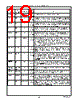
20 / 218 page  20 Signal/Pin Connection and Description www.national.com POR 159 APC Output Group 21 Power Off Request – This signal becomes active when an APC Switch Off event occurs, regardless of the fail-safe delay. Selection of edge or level for POR is via the APCR1 register of the APC. Selection of an output buffer is via GPIO22 output buffer control bits (in the Port 2 Output Type and Port 2 Pull-up Control registers described in Table 8-1 on page 170). See Section 4.3 on page 55. This signal is multiplexed with GPIO22. RD 33 ISA-Bus Input Group 1 I/O Read – An active low RD input signal indicates that the microprocessor has read data. RDATA 95 FDC Input Group 1 Read Data – This input signal holds raw serial data read from the Floppy Disk Drive (FDD). RI2,1 145, 135 UART1, APC Input Group 7 Ring Indicators (Modem) – When low, this signal indicates that a telephone ring signal has been received by the modem. The CPU can test the status of the RI modem status input signal by reading bit 6 (RI) of the Modem Status Register (MSR) for the appropriate serial channel. Bit 6 is the complement of the RI signal. Bit 2 (TERI) of the MSR indicates whether the RI input signal has changed from low to high since the previous reading of the MSR. When the TERI bit of the MSR is set, an interrupt is generated if modem status interrupts are enabled. When enabled, a high to low transition on RI1 or RI2 activates the ONCTL pin. The RI1 and RI2 pins each have an schmitt-trigger input buffer. RING 69 or 160 APC Input Group 7 Ring Indicator (APC) – Detection of an active low RING pulse or pulse train activates the ONCTL signal. The APC’s APCR2 register determines which pin the RING signal uses. The pins have a schmitt- trigger input buffer. RING is multiplexed on pin 69 with XDCS and on pin 160 with GPIO23. RTS2,1 146, 136 UART1, UART2 Output Group 17 Request to Send – When low, these output signals indicate to the modem or other data transfer device that the corresponding UART1 or UART2 is ready to exchange data. The RTS signal can be set active low by programming bit 1 (RTS) of the Modem Control Register (MCR) to a high level. A Master Reset (MR) sets RTS to inactive high. Loopback operation holds it inactive. RTS2 is multiplexed with CFG2. RTS1 is multiplexed with BADDR1. SELCS 77 Configuration Input Group 4 Select CSOUT – During reset, this signal is sampled into bit 1 of the SuperI/O Configuration 1 register (index 21h). A 40 K Ω internal pull-up resistor (or a 10 KΩ external pull-down resistor for National Semiconductor testing) controls this pin during reset. Do not pull this signal low during reset. This signal is multiplexed with GPIO21, IRSL2 and XD6. SIN2,1 147, 137 UART1, UART2 Input Group 1 Serial Input – This input signal receives composite serial data from the communications link (peripheral device, modem or other data transfer device.) SLCT 114 Parallel Port Input Group 2 Select – This input signal is set active high by the printer when the printer is selected. This pin is internally connected to a nominal 25 K Ω pull-down resistor. SLIN 118 Parallel Port I/O Group 13 Select Input – When this signal is active low it selects the printer. This signal is in TRI-STATE after a 0 is loaded into the corresponding control register bit. An external 4.7 K Ω pull-up resistor should be used. This signal is multiplexed with ASTRB. Signal/Pin Name Pin Number Module I/O and Group # Function |
|
Ligação URL |
| ALLDATASHEET é útil para você? [ DONATE ] |
Sobre Alldatasheet | Publicidade | Contato conosco | Privacy Policy | Link para a ficha técnica | roca de Link | Lista de Fabricantes All Rights Reserved©Alldatasheet.com |
| Russian : Alldatasheetru.com | Korean : Alldatasheet.co.kr | Spanish : Alldatasheet.es | French : Alldatasheet.fr | Italian : Alldatasheetit.com Portuguese : Alldatasheetpt.com | Polish : Alldatasheet.pl | Vietnamese : Alldatasheet.vn Indian : Alldatasheet.in | Mexican : Alldatasheet.com.mx | British : Alldatasheet.co.uk | New Zealand : Alldatasheet.co.nz |
|
Family Site : ic2ic.com |
icmetro.com |
 Portuguese ▼
 English
 Chinese
 German
 Japanese
 Russian
 Korean
 Spanish
 French
 Italian
 Portuguese
 Polish
 Vietnamese
 Indian
 Mexican
 British
 New Zealand