|
Os motores de busca de Datasheet de Componentes eletrônicos |
|
|
Os motores de busca de Datasheet de Componentes eletrônicos |
|
PC87307 Folha de dados(PDF) 66 Page - National Semiconductor (TI) |
|
|
|
|||||||||||||||||||||||||||||
PC87307 Folha de dados(HTML) 66 Page - National Semiconductor (TI) |
|
|
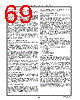
66 / 218 page  66 The Digital Floppy Disk Controller (FDC) (Logical Device 3) www.national.com 5.0 The Digital Floppy Disk Controller (FDC) (Logical Device 3) The Floppy Disk Controller (FDC) is suitable for all PC-AT, EISA, PS/2, and general purpose applications. DP8473 and N82077 software compatibility is provided. Key features in- clude a 16-byte FIFO, PS/2 diagnostic register support, per- pendicular recording mode, CMOS disk input and output logic, and a high performance Digital Data Separator (DDS). Figure 5-1 shows a functional block diagram of the FDC. The rest of this chapter describes the FDC functions, data transfer, the FDC registers, the phases of FDC commands, the result phase status registers and the FDC commands, in that order. 5.1 FDC FUNCTIONS FDC functions are enabled when the FDC Function Enable bit (bit 3) of the Function Enable Register 1 (FER1) at offset 00h in logical device 8 is set to 1. See Section 9.2.3 on page 173. The part is software compatible with the DP8473 and 82077 FDCs. Upon a power-on reset, the 16-byte FIFO is dis- abled. Also, the disk interface output signals are configured as active push-pull output signals, which are compatible with both CMOS input signals and open-collector, resistor- terminated, disk drive input signals. The FIFO can be enabled with the CONFIGURE command. The FIFO can be very useful at high data rates, with sys- tems that have a long DMA bus latency, or with multi-task- ing systems such as the EISA or MCA bus structures. The FDC supports all the DP8473 MODE command fea- tures as well as some additional features. These include control over the enabling of the FIFO for read and write op- erations, disabling burst mode for the FIFO, a bit that will configure the disk interface outputs as open-drain output signals, and programmability of the DENSEL output signal. 5.1.1 Microprocessor Interface The Floppy Disk Controller (FDC) receives commands, transfers data, and returns status information via an FDC microprocessor interface. This interface consists of the A9-3, AEN, RD, and WR signals, which access the chip for read and write operations; the data signals D7-0; the ad- dress lines A2-0, which select the appropriate register (see Table 5-1); an IRQ signal, and the DMA interface signals DRQ, DACK, and TC. 5.1.2 System Operation Modes The FDC operates in PC-AT or PS/2 drive mode, depending on the value of bit 2 of the SuperI/O Configuration 1 register at index 21h. See Section 2.4.3 on page 34. FIGURE 5-1. FDC Functional Block Diagram Internal Control and Data Bus Interface Logic Address Decoder DMA Enable Logic Main Status Register 16-Byte FIFO (MSR) PC8477B Micro-Engine and Timing/Control Logic Data Rate Selection Register (DSR) Configuration Control Register (CCR) 2 KB x 16 Micro-Code Status Register A Status Register B Digital Input Register (DIR) Digital Output Register (DOR) Write Precompen- Digital Data Separator (DDS) Disk Input and Output Logic DRATE0 DENSEL DIR DR1 HDSEL MTR0 sator MTR1 STEP WGATE WDATA DSKCHG INDEX RDATA TRK0 WP MSEN1,0 RD FDC Chip WR A2-0 Reset D7-0 FDC DMA TC FDC DMA Interrupt FDC Clock Select Acknowledge Request DR0 |
|
Ligação URL |
| ALLDATASHEET é útil para você? [ DONATE ] |
Sobre Alldatasheet | Publicidade | Contato conosco | Privacy Policy | Link para a ficha técnica | roca de Link | Lista de Fabricantes All Rights Reserved©Alldatasheet.com |
| Russian : Alldatasheetru.com | Korean : Alldatasheet.co.kr | Spanish : Alldatasheet.es | French : Alldatasheet.fr | Italian : Alldatasheetit.com Portuguese : Alldatasheetpt.com | Polish : Alldatasheet.pl | Vietnamese : Alldatasheet.vn Indian : Alldatasheet.in | Mexican : Alldatasheet.com.mx | British : Alldatasheet.co.uk | New Zealand : Alldatasheet.co.nz |
|
Family Site : ic2ic.com |
icmetro.com |
 Portuguese ▼
 English
 Chinese
 German
 Japanese
 Russian
 Korean
 Spanish
 French
 Italian
 Portuguese
 Polish
 Vietnamese
 Indian
 Mexican
 British
 New Zealand