|
Os motores de busca de Datasheet de Componentes eletrônicos |
|
|
Os motores de busca de Datasheet de Componentes eletrônicos |
|
PC87307 Folha de dados(PDF) 25 Page - National Semiconductor (TI) |
|
|
|
|||||||||||||||||||||||||||||
PC87307 Folha de dados(HTML) 25 Page - National Semiconductor (TI) |
|
|
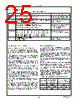
25 / 218 page  25 Configuration www.national.com 2.1.3 The Strap Pins TABLE 2-2. Strap Pins Pin Reset Configuration Affected CFG0 0 - FDC, KBC and RTC wake up inactive. 1 - FDC, KBC and RTC wake up active. Bit 0 of Activate registers (index 30h) of logical devices 0,2 and 3. CFG1 0 - No X-Bus Data Buffer. (See XDB pins multiplexing in Table 1-2.) 1 - X-Bus Data Buffer (XDB) enabled. Bit 4 of SuperI/O Configuration 1 register (index 21h). CFG3,2 00 - Clock source is 24 MHz fed via X1 pin. 01 - Reserved for CSOUT-NSC-Test fed via X1 pin. 10 - Clock source is 48 MHz fed via X1 pin. 11 - Clock source is 32.768 KHz with on-chip clock multiplier. Bits 2-0 of PMC2 register of Power Management (logical device 8) CFG2 affects bits 0 and 2. CFG3 affects bit 1. BADDR1,0 00 - Full PnP ISA, Wake in Wait For Key state. Index PnP ISA. 01 - Full PnP ISA, Wake in Wait For Key state. Index PnP ISA. 10 - PnP Motherboard, Wake in Config state. Index 015Ch. 11 - PnP Motherboard, Wake in Config state. Index 002Eh. Bits 1 and 0 of SuperI/O Configuration 2 register (index 22h) SELCS 0 - CSOUT-NSC-test on CS0 pin. 1 - CS0 on CS0 pin. Bit 1 of SuperI/O Configuration 1 register (index 21h). 2.2 SOFTWARE CONFIGURATION 2.2.1 Accessing the Configuration Registers Only two system I/O addresses are required to access any of the configuration registers. The Index and Data register pair is used to access registers for all read and write opera- tions. In a write operation, the target configuration register is iden- tified, based on a value that is loaded into the Index register. Then, the data to be written into the configuration register is transferred via the Data register. Similarly, for a read operation, first the source configuration register is identified, based on a value that is loaded into the Index register. Then, the data to be read is transferred via the Data register. Reading the Index register returns the last value loaded into the Index register. Reading the Data register returns the data in the configuration register pointed to by the Index register. If, during reset, the Base Address 1 (BADDR1) signal is low (0), the Index and Data registers are not accessible imme- diately after reset. As a result, all configuration registers of the part are also not accessible at this time. To access these registers, apply the PnP ISA protocol. If during reset, the Base Address 1 (BADDR1) signal is high (1), all configuration registers are accessible immediately after reset. It is up to the configuration software to guarantee no con- flicts between the registers of the active (enabled) logical devices, between IRQ signals and between DMA channels. If conflicts of this type occur, the results are unpredictable. To maintain compatibility with other SuperI/O‘s, the value of reserved bits may not be altered. Use read-modify-write. 2.2.2 Address Decoding In full Plug and Play mode, the addresses of the Index and Data registers that access the configuration registers are decoded using pins A11-0, according to the ISA Plug and Play specification. In Plug and Play Motherboard mode, the addresses of the Index and Data registers that access the configuration reg- isters are decoded using pins A15-1. Pin A0 distinguishes between these two registers. KBC and mouse register addresses are decoded using pins A1,0 and A15-3. Pin A2 distinguishes between the device registers. RTC/APC and Power Management (PM) register address- es are decoded using pins A15-1. PM has only five registers and only responds to accesses to those registers. FDC, UART, and GPIO register addresses are decoded us- ing pins A15-3. Parallel Port (PP) modes determine which pins are used for register addresses. In SPP mode, 14 pins are used to de- code Parallel Port (PP) base addresses. In ECP and EPP modes, 13 address pins are used. Table 2-3 shows which address pins are used in each mode. TABLE 2-3. Address Pins Used for Parallel Port PP Mode Pins Used to Decode Base Address Pins Used to Distinguish Registers SPP A15-2 A1,0 ECP A9-2 and A15-11 A1,0 and A10 EPP A15-3 A2-0 |
|
Ligação URL |
| ALLDATASHEET é útil para você? [ DONATE ] |
Sobre Alldatasheet | Publicidade | Contato conosco | Privacy Policy | Link para a ficha técnica | roca de Link | Lista de Fabricantes All Rights Reserved©Alldatasheet.com |
| Russian : Alldatasheetru.com | Korean : Alldatasheet.co.kr | Spanish : Alldatasheet.es | French : Alldatasheet.fr | Italian : Alldatasheetit.com Portuguese : Alldatasheetpt.com | Polish : Alldatasheet.pl | Vietnamese : Alldatasheet.vn Indian : Alldatasheet.in | Mexican : Alldatasheet.com.mx | British : Alldatasheet.co.uk | New Zealand : Alldatasheet.co.nz |
|
Family Site : ic2ic.com |
icmetro.com |
 Portuguese ▼
 English
 Chinese
 German
 Japanese
 Russian
 Korean
 Spanish
 French
 Italian
 Portuguese
 Polish
 Vietnamese
 Indian
 Mexican
 British
 New Zealand