|
Os motores de busca de Datasheet de Componentes eletrônicos |
|
|
Os motores de busca de Datasheet de Componentes eletrônicos |
|
AD9775 Folha de dados(PDF) 26 Page - Analog Devices |
|
|
|||||||||||||||||||||||||||||
AD9775 Folha de dados(HTML) 26 Page - Analog Devices |
|
|
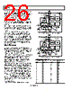
26 / 56 page  AD9775 Rev. E | Page 26 of 56 A transformer, such as the T1-1T from Mini-Circuits®, can also be used to convert a single-ended clock to differential. This method is used on the AD9775 evaluation board so that an external sine wave with no dc offset can be used as a differential clock. PECL/ECL drivers require varying termination networks, the details of which are left out of Figure 43 and Figure 44 but can be found in application notes such as AND8020/D from ON Semiconductor®. These networks depend on the assumed transmission line impedance and power supply voltage of the clock driver. Optimum performance of the AD9775 is achieved when the driver is placed very close to the AD9775 clock inputs, thereby negating any transmission line effects such as reflections due to mismatch. The quality of the clock and data input signals is important in achieving optimum performance. The external clock driver circuitry should provide the AD9775 with a low jitter clock input that meets the minimum/maximum logic levels while providing fast edges. Although fast clock edges help minimize any jitter that manifests itself as phase noise on a reconstructed waveform, the high gain bandwidth product of the AD9775 clock input comparator can tolerate differential sine wave inputs as low as 0.5 V p-p with minimal degradation of the output noise floor. PROGRAMMABLE PLL CLKIN can function either as an input data rate clock (PLL enabled) or as a DAC data rate clock (PLL disabled) according to the state of Address 0x02, Bit 7 in the SPI port register. The internal operation of the AD9775 clock circuitry in these two modes is illustrated in Figure 45 and Figure 46. The PLL clock multiplier and distribution circuitry produce the necessary internal synchronized 1×, 2×, 4×, and 8× clocks for the rising edge triggered latches, interpolation filters, modulators, and DACs. This circuitry consists of a phase detector, charge pump, voltage controlled oscillator (VCO), prescaler, clock distribution, and SPI port control. The charge pump, VCO, differential clock input buffer, phase detector, prescaler, and clock distribution are all powered from CLKVDD. PLL lock status is indicated by the logic signal at the DATACLK_PLL_LOCK pin, as well as by the status of Bit 1, Register 0x00. To ensure optimum phase noise performance from the PLL clock multiplier and distribution, CLKVDD should originate from a clean analog supply. Table 18 defines the minimum input data rates v s. the interpolation and PLL divider setting. If the input data rate drops below the defined minimum under these conditions, VCO noise may increase significantly. The VCO speed is a function of the input data rate, the interpolation rate, and the VCO prescaler, according to the following function: VCO Speed (MHz) = Input Data Rate (MHz) × Interpolation Rate × Prescaler AD9775 PLLVDD INPUT DATA LATCHES PLL_LOCK 1 = LOCK 0 = NO LOCK SPI PORT LPF CLK+ CLK– INTERPOLATION FILTERS, MODULATORS, AND DACS CLOCK DISTRIBUTION CIRCUITRY INTERPOLATION RATE CONTROL INTERNAL SPI CONTROL REGISTERS MODULATION RATE CONTROL PLL CONTROL (PLL ON) PLL DIVIDER (PRESCALER) CONTROL PRESCALER VCO PHASE DETECTOR CHARGE PUMP 2 1 48 Figure 45. PLL and Clock Circuitry with PLL Enabled AD9775 INPUT DATA LATCHES PLL_LOCK 1 = LOCK 0 = NO LOCK SPI PORT CLK+ CLK– INTERPOLATION FILTERS, MODULATORS, AND DACS CLOCK DISTRIBUTION CIRCUITRY INTERPOLATION RATE CONTROL INTERNAL SPI CONTROL REGISTERS MODULATION RATE CONTROL PLL CONTROL (PLL ON) PLL DIVIDER (PRESCALER) CONTROL PRESCALER VCO PHASE DETECTOR CHARGE PUMP 2 1 48 Figure 46. PLL and Clock Circuitry with PLL Disabled Table 18. PLL Optimization Interpolation Rate Divider Setting Minimum fDATA Maximum fDATA 1 1 32 160 1 2 16 160 1 4 8 112 1 8 4 56 2 1 24 160 2 2 12 112 2 4 6 56 2 8 3 28 4 1 24 100 4 2 12 56 4 4 6 28 4 8 3 14 8 1 24 50 8 2 12 28 8 4 6 14 8 8 3 7 |
|
Ligação URL |
| ALLDATASHEET é útil para você? [ DONATE ] |
Sobre Alldatasheet | Publicidade | Contato conosco | Privacy Policy | Link para a ficha técnica | roca de Link | Lista de Fabricantes All Rights Reserved©Alldatasheet.com |
| Russian : Alldatasheetru.com | Korean : Alldatasheet.co.kr | Spanish : Alldatasheet.es | French : Alldatasheet.fr | Italian : Alldatasheetit.com Portuguese : Alldatasheetpt.com | Polish : Alldatasheet.pl | Vietnamese : Alldatasheet.vn Indian : Alldatasheet.in | Mexican : Alldatasheet.com.mx | British : Alldatasheet.co.uk | New Zealand : Alldatasheet.co.nz |
|
Family Site : ic2ic.com |
icmetro.com |
 Portuguese ▼
 English
 Chinese
 German
 Japanese
 Russian
 Korean
 Spanish
 French
 Italian
 Portuguese
 Polish
 Vietnamese
 Indian
 Mexican
 British
 New Zealand