|
Os motores de busca de Datasheet de Componentes eletrônicos |
|
|
Os motores de busca de Datasheet de Componentes eletrônicos |
|
AD9775 Folha de dados(PDF) 43 Page - Analog Devices |
|
|
|||||||||||||||||||||||||||||
AD9775 Folha de dados(HTML) 43 Page - Analog Devices |
|
|
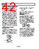
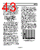
43 / 56 page  AD9775 Rev. E | Page 43 of 56 DIFFERENTIAL COUPLING USING AN OP AMP An op amp can also be used to perform a differential-to-single- ended conversion, as shown in Figure 99. This has the added benefit of providing signal gain as well. In Figure 99, the AD9775 is configured with two equal load resistors, RLOAD, of 25 Ω. The differential voltage developed across IOUTA and IOUTB is converted to a single-ended signal via the differential op amp configuration. An optional capacitor can be installed across IOUTA and IOUTB, forming a real pole in a low-pass filter. The addition of this capacitor also enhances the op amp distortion performance by preventing the DAC fast slewing output from overloading the input of the op amp. IOUTA IOUTB COPT ROPT 225 Ω DAC 225 Ω 225 Ω 500 Ω 500 Ω 25 Ω 25 Ω AVDD AD8021 Figure 99. Op Amp-Coupled Output Circuit The common-mode (and second-order distortion) rejection of this configuration is typically determined by the resistor matching. The op amp used must operate from a dual supply because its output is approximately ±1.0 V. A high speed amplifier, such as the AD8021, capable of preserving the differential performance of the AD9775 while meeting other system level objectives (such as cost and power) is recommended. The op amp differential gain, its gain setting resistor values, and full-scale output swing capabilities should all be considered when optimizing this circuit. ROPT is only necessary if level shifting is required on the op amp output. In Figure 99, AVDD, which is the positive analog supply for both the AD9775 and the op amp, is also used to level shift the differential output of the AD9775 to midsupply, that is, AVDD/2. INTERFACING THE AD9775 WITH THE AD8345 QUADRATURE MODULATOR The AD9775 architecture was defined to operate in a transmit signal chain using an image reject architecture. A quadrature modulator is also required in this application and should be designed to meet the output characteristics of the DAC as much as possible. The AD8345 from Analog Devices meets many of the requirements for interfacing with the AD9775. As with any DAC output interface, there are a number of issues that have to be resolved. The following sections list some of these issues. DAC Compliance Voltage/Input Common-Mode Range The dynamic range of the AD9775 is optimal when the DAC outputs swing between ±1.0 V. The input common-mode range of the AD8345, at 0.7 V, allows optimum dynamic range to be achieved in both components. Gain/Offset Adjust The matching of the DAC output to the common-mode input of the AD8345 allows the two components to be dc-coupled, with no level shifting necessary. The combined voltage offset of the two parts can therefore be compensated for via the AD9775 programmable offset adjust. This allows excellent LO cancella- tion at the AD8345 output. The programmable gain adjust allows for optimal image rejection as well. The AD9775 evaluation board includes an AD8345 and recommended interface (Figure 104 and Figure 105). On the output of the AD9775, R9 and R10 convert the DAC output current to a voltage. R16 may be used to do a slight common- mode shift if necessary. The (now voltage) signal is applied to a low-pass reconstruction filter to reject DAC images. The components installed on the AD9775 provide a 35 MHz cutoff but may be changed to fit the application. A balun (Mini- Circuits ADTL1-12) is used to cross the ground plane boundary to the AD8345. Another balun (Mini-Circuits ETC1-1-13) is used to couple the LO input of the AD8345. The interface requires a low ac impedance return path from the AD8345, so a single connection between the AD9775 and AD8345 ground planes is recommended. The performance of the AD9775 and AD8345 in an image reject transmitter, reconstructing three W-CDMA carriers, can be seen in Figure 100. The LO of the AD8345 in this application is 800 MHz. Image rejection (50 dB) and LO feedthrough (−78 dBFS) have been optimized with the programmable features of the AD9775. The average output power of the digital waveform for this test was set to −15 dBFS to account for the peak-to-average ratio of the W-CDMA signal. –100 –90 –80 –70 –60 –50 –40 –30 –20 –10 0 FREQUENCY (MHz) 782.5 762.5 802.5 822.5 842.5 Figure 100. AD9775/AD8345 Synthesizing a Three-Carrier W-CDMA Signal at an LO of 800 MHz |
|
Ligação URL |
| ALLDATASHEET é útil para você? [ DONATE ] |
Sobre Alldatasheet | Publicidade | Contato conosco | Privacy Policy | Link para a ficha técnica | roca de Link | Lista de Fabricantes All Rights Reserved©Alldatasheet.com |
| Russian : Alldatasheetru.com | Korean : Alldatasheet.co.kr | Spanish : Alldatasheet.es | French : Alldatasheet.fr | Italian : Alldatasheetit.com Portuguese : Alldatasheetpt.com | Polish : Alldatasheet.pl | Vietnamese : Alldatasheet.vn Indian : Alldatasheet.in | Mexican : Alldatasheet.com.mx | British : Alldatasheet.co.uk | New Zealand : Alldatasheet.co.nz |
|
Family Site : ic2ic.com |
icmetro.com |
 Portuguese ▼
 English
 Chinese
 German
 Japanese
 Russian
 Korean
 Spanish
 French
 Italian
 Portuguese
 Polish
 Vietnamese
 Indian
 Mexican
 British
 New Zealand