|
Os motores de busca de Datasheet de Componentes eletrônicos |
|
|
Os motores de busca de Datasheet de Componentes eletrônicos |
|
AD9775 Folha de dados(PDF) 36 Page - Analog Devices |
|
|
|||||||||||||||||||||||||||||
AD9775 Folha de dados(HTML) 36 Page - Analog Devices |
|
|
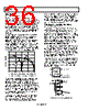
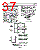
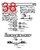
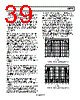
36 / 56 page  AD9775 Rev. E | Page 36 of 56 ZERO STUFFING (Control Register 0x01, Bit 3) As shown in Figure 75, a 0 or null in the output frequency response of the DAC (after interpolation, modulation, and DAC reconstruction) occurs at the final DAC sample rate (fDAC). This is due to the inherent sin(x)/x roll-off response in the digital-to- analog conversion. In applications where the desired frequency content is below fDAC/2, this may not be a problem. Note that at fDAC/2 the loss due to sin(x)/x is 4 dB. In direct RF applications, this roll-off may be problematic due to the increased pass-band amplitude variation as well as the reduced amplitude of the desired signal. Consider an application where the digital data into the AD9775 represents a baseband signal around fDAC/4 with a pass band of fDAC/10. The reconstructed signal out of the AD9775 would experience only a 0.75 dB amplitude variation over its pass band. However, the image of the same signal occurring at 3 × fDAC/4 suffers from a pass-band flatness variation of 3.93 dB. This image may be the desired signal in an IF application using one of the various modulation modes in the AD9775. This roll-off of image frequencies can be seen in Figure 59 to Figure 74, where the effect of the interpolation and modulation rate is apparent as well. –50 –40 –30 –20 –10 0 10 fOUT, NORMALIZED TO fDATA WITH ZERO STUFFING DISABLED (Hz) 0.5 0 1.0 1.5 2.0 ZERO STUFFING ENABLED ZERO STUFFING DISABLED Figure 75. Effect of Zero Stuffing on DAC’s sin(x)/x Response To improve upon the pass-band flatness of the desired image, the zero stuffing mode can be enabled by setting the control register bit to Logic 1. This option increases the ratio of fDAC/fDATA by a factor of 2 by doubling the DAC sample rate and inserting a midscale sample (that is, 1000 0000 0000 0000) after every data sample originating from the interpolation filter. This is important as it affects the PLL divider ratio needed to keep the VCO within its optimum speed range. Note that the zero stuffing takes place in the digital signal chain at the output of the digital modulator before the DAC. The net effect is to increase the DAC output sample rate by a factor of 2× with the 0 in the sin(x)/x DAC transfer function occurring at twice the original frequency. A 6 dB loss in amplitude at low frequencies is also evident (see Figure 75). Note that the zero-stuffing option by itself does not change the location of the images but rather their amplitude, pass-band flatness, and relative weighting. For instance, in the previous example, the pass-band amplitude flatness of the image at 3 × fDATA/4 improved to +0.59 dB while the signal level increased slightly from −10.5 dBFS to −8.1 dBFS. INTERPOLATING (COMPLEX MIX MODE) (Control Register 0x01, Bit 2) In the complex mix mode, the two digital modulators on the AD9775 are coupled to provide a complex modulation function. In conjunction with an external quadrature modulator, this complex modulation can be used to realize a transmit image rejection architecture. The complex modulation function can be programmed for e+jωt or e−jωt to give upper or lower image rejection. As in the real modulation mode, the modulation frequency ω can be programmed via the SPI port for fDAC/2, fDAC/4, and fDAC/8, where fDAC represents the DAC output rate. OPERATIONS ON COMPLEX SIGNALS Truly complex signals cannot be realized outside of a computer simulation. However, two data channels, both consisting of real data, can be defined as the real and imaginary components of a complex signal. I (real) and Q (imaginary) datapaths are often defined this way. By using the architecture defined in Figure 76, a system can be realized that operates on complex signals, giving a complex (real and imaginary) output. If a complex modulation function (e+jωt) is desired, the real and imaginary components of the system correspond to the real and imaginary components of e+jωt or cosωt and sinωt. As Figure 77 shows, the complex modulation function can be realized by applying these components to the structure of the complex system defined in Figure 76. a(t) = (c + jd) b(t) c(t) × b(t) + d × b(t) b(t) × a(t) + c × b(t) INPUT OUTPUT INPUT OUTPUT COMPLEX FILTER IMAGINARY Figure 76. Realization of a Complex System INPUT (REAL) OUTPUT (REAL) OUTPUT (IMAGINARY) INPUT (IMAGINARY) 90 ° e–jωt = COS ωt + jSINωt Figure 77. Implementation of a Complex Modulator |
|
Ligação URL |
| ALLDATASHEET é útil para você? [ DONATE ] |
Sobre Alldatasheet | Publicidade | Contato conosco | Privacy Policy | Link para a ficha técnica | roca de Link | Lista de Fabricantes All Rights Reserved©Alldatasheet.com |
| Russian : Alldatasheetru.com | Korean : Alldatasheet.co.kr | Spanish : Alldatasheet.es | French : Alldatasheet.fr | Italian : Alldatasheetit.com Portuguese : Alldatasheetpt.com | Polish : Alldatasheet.pl | Vietnamese : Alldatasheet.vn Indian : Alldatasheet.in | Mexican : Alldatasheet.com.mx | British : Alldatasheet.co.uk | New Zealand : Alldatasheet.co.nz |
|
Family Site : ic2ic.com |
icmetro.com |
 Portuguese ▼
 English
 Chinese
 German
 Japanese
 Russian
 Korean
 Spanish
 French
 Italian
 Portuguese
 Polish
 Vietnamese
 Indian
 Mexican
 British
 New Zealand