|
Os motores de busca de Datasheet de Componentes eletrônicos |
|
|
Os motores de busca de Datasheet de Componentes eletrônicos |
|
AD9775 Folha de dados(PDF) 11 Page - Analog Devices |
|
|
|||||||||||||||||||||||||||||
AD9775 Folha de dados(HTML) 11 Page - Analog Devices |
|
|
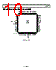
11 / 56 page  AD9775 Rev. E | Page 11 of 56 Table 9. Pin Function Descriptions Pin No. Mnemonic Description 1, 3 CLKVDD Clock Supply Voltage. 2 LPF PLL Loop Filter. 4, 7 CLKGND Clock Supply Common. 5 CLK+ Differential Clock Input. 6 CLK− Differential Clock Input. 8 DATACLK/PLL_LOCK With the PLL enabled, this pin indicates the state of the PLL. A read of a Logic 1 indicates the PLL is in the locked state. Logic 0 indicates the PLL has not achieved lock. This pin may also be programmed to act as either an input or output (Address 02h, Bit 3) DATACLK signal running at the input data rate. 9, 17, 25, 35, 44, 52 DGND Digital Common. 10, 18, 26, 36, 43, 51 DVDD Digital Supply Voltage. 11 to 16, 19 to 24, 27, 28 P1B13 (MSB) to P1B0 (LSB) Port 1 Data Inputs. 29, 30, 49, 50 NC No Connect. 31 IQSEL/P2B13 (MSB) In one-port mode, IQSEL = 1 followed by a rising edge of the differential input clock latches the data into the I channel input register. IQSEL = 0 latches the data into the Q channel input register. In two-port mode, this pin becomes the Port 2 MSB. 32 ONEPORTCLK/P2B12 With the PLL disabled and the AD9775 in one-port mode, this pin becomes a clock output that runs at twice the input data rate of the I and Q channels. This allows the AD9775 to accept and demux interleaved I and Q data to the I and Q input registers. 33, 34, 37 to 42, 45 to 48 P2B11 to P2B0 (LSB) Port 2 Data Inputs. 53 SPI_SDO In the case where SDIO is an input, SDO acts as an output. When SDIO becomes an output, SDO enters a High-Z state. This pin can also be used as an output for the data rate clock. For more information, see the Two-Port Data Input Mode section. 54 SPI_SDIO Bidirectional Data Pin. Data direction is controlled by Bit 7 of Register Address 0x00. The default setting for this bit is 0, which sets SDIO as an input. 55 SPI_CLK Data input to the SPI port is registered on the rising edge of SPI_CLK. Data output on the SPI port is registered on the falling edge. 56 SPI_CSB Chip Select/SPI Data Synchronization. On momentary logic high, resets SPI port logic and initializes instruction cycle. 57 RESET Logic 1 resets all of the SPI port registers, including Address 0x00, to their default values. A software reset can also be done by writing a Logic 1 to SPI Register 00h, Bit 5. However, the software reset has no effect on the bit in Address 0x00. 58 REFIO Reference Output, 1.2 V Nominal. 59 FSADJ2 Full-Scale Current Adjust, Q Channel. 60 FSADJ1 Full-Scale Current Adjust, I Channel. 61, 63, 65, 76, 78, 80 AVDD Analog Supply Voltage. 62, 64, 66, 67, 70, 71, 74, 75, 77, 79 AGND Analog Common. 68, 69 IOUTB2, IOUTA2 Differential DAC Current Outputs, Q Channel. 72, 73 IOUTB1, IOUTA1 Differential DAC Current Outputs, I Channel. |
|
Ligação URL |
| ALLDATASHEET é útil para você? [ DONATE ] |
Sobre Alldatasheet | Publicidade | Contato conosco | Privacy Policy | Link para a ficha técnica | roca de Link | Lista de Fabricantes All Rights Reserved©Alldatasheet.com |
| Russian : Alldatasheetru.com | Korean : Alldatasheet.co.kr | Spanish : Alldatasheet.es | French : Alldatasheet.fr | Italian : Alldatasheetit.com Portuguese : Alldatasheetpt.com | Polish : Alldatasheet.pl | Vietnamese : Alldatasheet.vn Indian : Alldatasheet.in | Mexican : Alldatasheet.com.mx | British : Alldatasheet.co.uk | New Zealand : Alldatasheet.co.nz |
|
Family Site : ic2ic.com |
icmetro.com |
 Portuguese ▼
 English
 Chinese
 German
 Japanese
 Russian
 Korean
 Spanish
 French
 Italian
 Portuguese
 Polish
 Vietnamese
 Indian
 Mexican
 British
 New Zealand