|
Os motores de busca de Datasheet de Componentes eletrônicos |
|
|
Os motores de busca de Datasheet de Componentes eletrônicos |
|
AD9775 Folha de dados(PDF) 44 Page - Analog Devices |
|
|
|||||||||||||||||||||||||||||
AD9775 Folha de dados(HTML) 44 Page - Analog Devices |
|
|
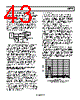
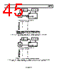
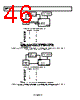
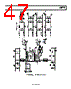
44 / 56 page  AD9775 Rev. E | Page 44 of 56 EVALUATION BOARD The AD9775 evaluation board allows easy configuration of the various modes, programmable via the SPI port. Software is available for programming the SPI port from PCs running Windows® 95, Windows 98, or Windows NT®/2000. The evaluation board also contains an AD8345 quadrature modulator and support circuitry that allows the user to optimally configure the AD9775 in an image reject transmit signal chain. Figure 101 to Figure 104 show how to configure the evaluation board in the one-port and two-port input modes with the PLL enabled and disabled. Refer to Figure 105 to Figure 114, the schematics, and the layout for the AD9775 evaluation board for the jumper locations described in the DAC Single-Ended Outputs section. The AD9775 outputs can be configured for various applications by referring to the following instructions. DAC Single-Ended Outputs Remove Transformers T2 and T3. Solder jumper links JP4 or JP28 to look at the DAC1 outputs. Solder jumper links JP29 or JP30 to look at the DAC2 outputs. Jumper 8 and Jumper 13 to Jumper 17 should remain unsoldered. Jumper JP35 to Jumper JP38 can be used to ground one of the DAC outputs while the other is measured single ended. Optimum single-ended distortion performance is typically achieved in this manner. The outputs are taken from S3 and S4. DAC Differential Outputs Transformers T2 and T3 should be in place. Note that the lower band of operation for these transformers is 300 kHz to 500 kHz. Jumper 4, Jumper 8, Jumper 13 to Jumper 17, and Jumper 28 to Jumper 30 should remain unsoldered. The outputs are taken from S3 and S4. Using the AD8345 Remove Transformers T2 and T3. Jumper JP4 and Jumper 28 to Jumper 30 should remain unsoldered. Jumper 13 to Jumper 16 should be soldered. The desired components for the low-pass interface filter L6, L7, C55, and C81 should be in place. The LO drive is connected to the AD8345 via J10 and the balun T4, and the AD8345 output is taken from J9. |
|
Ligação URL |
| ALLDATASHEET é útil para você? [ DONATE ] |
Sobre Alldatasheet | Publicidade | Contato conosco | Privacy Policy | Link para a ficha técnica | roca de Link | Lista de Fabricantes All Rights Reserved©Alldatasheet.com |
| Russian : Alldatasheetru.com | Korean : Alldatasheet.co.kr | Spanish : Alldatasheet.es | French : Alldatasheet.fr | Italian : Alldatasheetit.com Portuguese : Alldatasheetpt.com | Polish : Alldatasheet.pl | Vietnamese : Alldatasheet.vn Indian : Alldatasheet.in | Mexican : Alldatasheet.com.mx | British : Alldatasheet.co.uk | New Zealand : Alldatasheet.co.nz |
|
Family Site : ic2ic.com |
icmetro.com |
 Portuguese ▼
 English
 Chinese
 German
 Japanese
 Russian
 Korean
 Spanish
 French
 Italian
 Portuguese
 Polish
 Vietnamese
 Indian
 Mexican
 British
 New Zealand