|
Os motores de busca de Datasheet de Componentes eletrônicos |
|
|
Os motores de busca de Datasheet de Componentes eletrônicos |
|
AD9775 Folha de dados(PDF) 21 Page - Analog Devices |
|
|
|||||||||||||||||||||||||||||
AD9775 Folha de dados(HTML) 21 Page - Analog Devices |
|
|
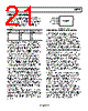
21 / 56 page  AD9775 Rev. E | Page 21 of 56 FUNCTIONAL DESCRIPTION The AD9775 dual interpolating DAC consists of two data channels that can be operated independently or coupled to form a complex modulator in an image reject transmit architecture. Each channel includes three FIR filters, making the AD9775 capable of 2×, 4×, or 8× interpolation. High speed input and output data rates can be achieved within the following limitations. Table 15. Interpolation Rate (MSPS) Input Data Rate (MSPS) DAC Sample Rate (MSPS) 1× 160 160 2× 160 320 4× 100 400 8× 50 400 Both data channels contain a digital modulator capable of mixing the data stream with an LO of fDAC/2, fDAC/4, or fDAC/8, where fDAC is the output data rate of the DAC. A zero-stuffing feature is also included and can be used to improve pass-band flatness for signals being attenuated by the sin(x)/x characteristic of the DAC output. The speed of the AD9775, combined with the digital modulation capability, enables direct IF conversion architectures at 70 MHz and higher. The digital modulators on the AD9775 can be coupled to form a complex modulator. By using this feature with an external analog quadrature modulator, such as the Analog Devices AD8345, an image rejection architecture can be enabled. To optimize the image rejection capability, as well as LO feed- through in this architecture, the AD9775 offers programmable (via the SPI port) gain and offset adjust for each DAC. Also included on the AD9775 are a phase-locked loop (PLL) clock multiplier and a 1.20 V band gap voltage reference. With the PLL enabled, a clock applied to the CLK+/CLK− inputs is frequency multiplied internally and generates all necessary internal synchronization clocks. Each 14-bit DAC provides two complementary current outputs whose full-scale currents can be determined either from a single external resistor or independently from two separate resistors (see the 1R/2R Mode section). The AD9775 features a low jitter, differential clock input that provides excellent noise rejection while accepting a sine or square wave input. Separate voltage supply inputs are provided for each functional block to ensure optimum noise and distortion performance. Sleep and power-down modes can be used to turn off the DAC output current (sleep) or the entire digital and analog sections (power-down) of the chip. An SPI-compliant serial port is used to program the many features of the AD9775. Note that in power-down mode, the SPI port is the only section of the chip still active. SDO (PIN 53) SDIO (PIN 54) SPI_CLK (PIN 55) CSB (PIN 56) AD9775 SPI PORT INTERFACE Figure 32. SPI Port Interface SERIAL INTERFACE FOR REGISTER CONTROL The AD9775 serial port is a flexible, synchronous serial communications port that allows easy interface to many industry-standard microcontrollers and microprocessors. The serial I/O is compatible with most synchronous transfer formats, including both the Motorola SPI and Intel SSR protocols. The interface allows read/write access to all registers that configure the AD9775. Single- or multiple-byte transfers are supported, as well as MSB-first or LSB-first transfer formats. The AD9775 serial interface port can be configured as a single pin I/O (SDIO) or two unidirectional pins for I/O (SDIO/SDO). GENERAL OPERATION OF THE SERIAL INTERFACE There are two phases to a communication cycle with the AD9775. Phase 1 is the instruction cycle, which is the writing of an instruction byte into the AD9775 coincident with the first eight SCLK rising edges. The instruction byte provides the AD9775 serial port controller with information regarding the data transfer cycle, which is Phase 2 of the communication cycle. The Phase 1 instruction byte defines whether the upcoming data transfer is read or write, the number of bytes in the data transfer, and the starting register address for the first byte of the data transfer. The first eight SCLK rising edges of each communication cycle are used to write the instruction byte into the AD9775. A Logic 1 on the SPI_CSB pin, followed by a logic low, resets the SPI port timing to the initial state of the instruction cycle. This is true regardless of the present state of the internal registers or the other signal levels present at the inputs to the SPI port. If the SPI port is in the middle of an instruction cycle or a data transfer cycle, none of the present data is written. The remaining SCLK edges are for Phase 2 of the communication cycle. Phase 2 is the actual data transfer between the AD9775 and the system controller. Phase 2 of the communication cycle is a transfer of one to four data bytes as determined by the instruction byte. Typically, using one multibyte transfer is the preferred method. However, single byte data transfers are useful to reduce CPU overhead when register access requires one byte only. Registers change immediately upon writing to the last bit of each transfer byte. |
|
Ligação URL |
| ALLDATASHEET é útil para você? [ DONATE ] |
Sobre Alldatasheet | Publicidade | Contato conosco | Privacy Policy | Link para a ficha técnica | roca de Link | Lista de Fabricantes All Rights Reserved©Alldatasheet.com |
| Russian : Alldatasheetru.com | Korean : Alldatasheet.co.kr | Spanish : Alldatasheet.es | French : Alldatasheet.fr | Italian : Alldatasheetit.com Portuguese : Alldatasheetpt.com | Polish : Alldatasheet.pl | Vietnamese : Alldatasheet.vn Indian : Alldatasheet.in | Mexican : Alldatasheet.com.mx | British : Alldatasheet.co.uk | New Zealand : Alldatasheet.co.nz |
|
Family Site : ic2ic.com |
icmetro.com |
 Portuguese ▼
 English
 Chinese
 German
 Japanese
 Russian
 Korean
 Spanish
 French
 Italian
 Portuguese
 Polish
 Vietnamese
 Indian
 Mexican
 British
 New Zealand