|
Os motores de busca de Datasheet de Componentes eletrônicos |
|
|
Os motores de busca de Datasheet de Componentes eletrônicos |
|
AD9775 Folha de dados(PDF) 42 Page - Analog Devices |
|
|
|||||||||||||||||||||||||||||
AD9775 Folha de dados(HTML) 42 Page - Analog Devices |
|
|
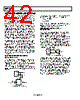
42 / 56 page  AD9775 Rev. E | Page 42 of 56 APPLYING THE OUTPUT CONFIGURATIONS The following sections illustrate typical output configurations for the AD9775. Unless otherwise noted, it is assumed that IOUTFS is set to a nominal 20 mA. For applications requiring optimum dynamic performance, a differential output configu- ration is suggested. A simple differential output may be achieved by converting IOUTA and IOUTB to a voltage output by terminating them to AGND via equal value resistors. This type of configuration may be useful when driving a differential voltage input device such as a modulator. If a conversion to a single-ended signal is desired and the application allows for ac coupling, an RF transformer may be useful, or if power gain is required, an op amp may be used. The transformer configu- ration provides optimum high frequency noise and distortion performance. The differential op amp configuration is suitable for applications requiring dc coupling, signal gain, and/or level shifting within the bandwidth of the chosen op amp. A single-ended output is suitable for applications requiring a unipolar voltage output. A positive unipolar output voltage results if IOUTA and/or IOUTB is connected to a load resistor, RLOAD, referred to AGND. This configuration is most suitable for a single-supply system requiring a dc-coupled, ground-referred output voltage. Alternatively, an amplifier could be configured as an I-V converter, thus converting IOUTA or IOUTB into a negative unipolar voltage. This configuration provides the best DAC dc linearity as IOUTA or IOUTB are maintained at ground or virtual ground. UNBUFFERED DIFFERENTIAL OUTPUT, EQUIVALENT CIRCUIT In many applications, it may be necessary to understand the equivalent DAC output circuit. This is especially useful when designing output filters or when driving inputs with finite input impedances. Figure 97 illustrates the output of the AD9775 and the equivalent circuit. A typical application where this information may be useful is when designing an interface filter between the AD9775 and Analog Devices’ AD8345 quadrature modulator. IOUTA IOUTB VOUT+ VOUT (DIFFERENTIAL) VSOURCE = IOUTFS × (RA + RB) p-p VOUT– RA + RB Figure 97. DAC Output Equivalent Circuit For the typical situation, where IOUTFS = 20 mA and RA and RB both equal 50 Ω, the equivalent circuit values become 2 = SOURCE V V p-p Ω 100 = OUT R Note that the output impedance of the AD9775 DAC itself is greater than 100 kΩ and typically has no effect on the impedance of the equivalent output circuit. DIFFERENTIAL COUPLING USING A TRANSFORMER An RF transformer can be used to perform a differential-to- single-ended signal conversion, as shown in Figure 98. A dif- ferentially coupled transformer output provides the optimum distortion performance for output signals whose spectral content lies within the transformer’s pass band. An RF transformer, such as the Mini-Circuits T1-1T, provides excellent rejection of common-mode distortion (that is, even-order harmonics) and noise over a wide frequency range. It also provides electrical isolation and the ability to deliver twice the power to the load. Transformers with different impedance ratios can also be used for impedance matching purposes. MINI-CIRCUITS T1-1T RLOAD IOUTA IOUTB DAC Figure 98. Transformer-Coupled Output Circuit The center tap on the primary side of the transformer must be connected to AGND to provide the necessary dc current path for both IOUTA and IOUTB. The complementary voltages appearing at IOUTA and IOUTB (that is, VOUTA and VOUTB) swing symmetrically around AGND and should be maintained within the specified output compliance range of the AD9775. A differential resistor, RDIFF, can be inserted in applications where the output of the transformer is connected to the load, RLOAD, via a passive reconstruction filter or cable. RDIFF is determined by the transformer’s impedance ratio and provides the proper source termination that results in a low VSWR. Note that approxi- mately half the signal power dissipates across RDIFF. |
|
Ligação URL |
| ALLDATASHEET é útil para você? [ DONATE ] |
Sobre Alldatasheet | Publicidade | Contato conosco | Privacy Policy | Link para a ficha técnica | roca de Link | Lista de Fabricantes All Rights Reserved©Alldatasheet.com |
| Russian : Alldatasheetru.com | Korean : Alldatasheet.co.kr | Spanish : Alldatasheet.es | French : Alldatasheet.fr | Italian : Alldatasheetit.com Portuguese : Alldatasheetpt.com | Polish : Alldatasheet.pl | Vietnamese : Alldatasheet.vn Indian : Alldatasheet.in | Mexican : Alldatasheet.com.mx | British : Alldatasheet.co.uk | New Zealand : Alldatasheet.co.nz |
|
Family Site : ic2ic.com |
icmetro.com |
 Portuguese ▼
 English
 Chinese
 German
 Japanese
 Russian
 Korean
 Spanish
 French
 Italian
 Portuguese
 Polish
 Vietnamese
 Indian
 Mexican
 British
 New Zealand