|
Os motores de busca de Datasheet de Componentes eletrônicos |
|
|
Os motores de busca de Datasheet de Componentes eletrônicos |
|
AD9775 Folha de dados(PDF) 25 Page - Analog Devices |
|
|
|||||||||||||||||||||||||||||
AD9775 Folha de dados(HTML) 25 Page - Analog Devices |
|
|
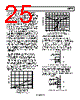
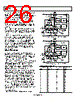
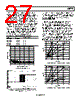
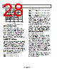
25 / 56 page  AD9775 Rev. E | Page 25 of 56 The offset control defines a small current that can be added to IOUTA or IOUTB (not both) on the IDAC and QDAC. The selection of which IOUT this offset current is directed toward is programmable via Register 0x08, Bit 7 (IDAC) and Register 0x0C, Bit 7 (QDAC). Figure 41 shows the scale of the offset current that can be added to one of the complementary outputs on the IDAC and QDAC. Offset control can be used for suppression of LO leakage resulting from modulation of dc signal components. If the AD9775 is dc- coupled to an external modulator, this feature can be used to cancel the output offset on the AD9775 as well as the input offset on the modulator. Figure 42 shows a typical example of the effect that the offset control has on LO suppression. In Figure 42, the negative scale represents an offset added to IOUTB, while the positive scale represents an offset added to IOUTA of the respective DAC. Offset Register 1 corresponds to IDAC, while Offset Register 2 corresponds to QDAC. Figure 42 represents the AD9775 synthesizing a complex signal that is then dc-coupled to an AD8345 quadrature modulator with an LO of 800 MHz. The dc coupling allows the input offset of the AD8345 to be calibrated out as well. The LO suppression at the AD8345 output was opti- mized first by adjusting Offset Register 1 in the AD9775. When an optimal point was found (roughly Code 54), this code was held in Offset Register 1, and Offset Register 2 was adjusted. The resulting LO suppression is 70 dBFS. These are typical numbers; the specific code for optimization varies from part to part. 1R/2R MODE In 2R mode, the reference current for each channel is set independently by the FSADJ resistor on that channel. The AD9775 can be programmed to derive its reference current from a single resistor on Pin 60 by placing the part into 1R mode. The transfer functions in Equation 1 are valid for 2R mode. In 1R mode, the current developed in the single FSADJ resistor is split equally between the two channels. The result is that in 1R mode, a scale factor of 1/2 must be applied to the formulas in Equation 1. The full-scale DAC current in 1R mode can still be set to as high as 20 mA by using the internal 1.2 V reference and a 950 Ω resistor instead of the 1.9 kΩ resistor typically used in the 2R mode. 0 1 2 3 4 5 0 COARSE GAIN REGISTER CODE (ASSUMING RSET1, RSET2 = 1.9k Ω) 2R MODE 1R MODE 0 200 400 600 800 1000 Figure 41. DAC Output Offset Current –80 –70 –60 –50 –40 –30 –20 –10 0 0 –256 –768 –512 –1024 256 512 768 1024 DAC1, DAC2 (OFFSET REGISTER CODES) OFFSET REGISTER 1 ADJUSTED OFFSET REGISTER 2 ADJUSTED, WITH OFFSET REGISTER 1 SET TO OPTIMIZED VALUE Figure 42. Offset Adjust Control, Effect on LO Suppression CLOCK INPUT CONFIGURATIONS The clock inputs to the AD9775 can be driven differentially or single-ended. The internal clock circuitry has supply and ground (CLKVDD, CLKGND) separate from the other supplies on the chip to minimize jitter from internal noise sources. Figure 43 shows the AD9775 driven from a single-ended clock source. The CLK+/CLK− pins form a differential input (CLKIN) so that the statically terminated input must be dc- biased to the midswing voltage level of the clock driven input. AD9775 RSERIES CLK+ CLK– 0.1 μF CLKVDD CLKGND VTHRESHOLD Figure 43. Single-Ended Clock Driving Clock Inputs A configuration for differentially driving the clock inputs is given in Figure 44. DC-blocking capacitors can be used to couple a clock driver output whose voltage swings exceed CLKVDD or CLKGND. If the driver voltage swings are within the supply range of the AD9775, the dc-blocking capacitors and bias resistors are not necessary. AD9775 CLK+ 0.1 μF 0.1 μF 0.1 μF 1k Ω 1k Ω 1k Ω 1k Ω ECL/PECL CLK– CLKVDD CLKGND Figure 44. Differential Clock Driving Clock Inputs |
|
Ligação URL |
| ALLDATASHEET é útil para você? [ DONATE ] |
Sobre Alldatasheet | Publicidade | Contato conosco | Privacy Policy | Link para a ficha técnica | roca de Link | Lista de Fabricantes All Rights Reserved©Alldatasheet.com |
| Russian : Alldatasheetru.com | Korean : Alldatasheet.co.kr | Spanish : Alldatasheet.es | French : Alldatasheet.fr | Italian : Alldatasheetit.com Portuguese : Alldatasheetpt.com | Polish : Alldatasheet.pl | Vietnamese : Alldatasheet.vn Indian : Alldatasheet.in | Mexican : Alldatasheet.com.mx | British : Alldatasheet.co.uk | New Zealand : Alldatasheet.co.nz |
|
Family Site : ic2ic.com |
icmetro.com |
 Portuguese ▼
 English
 Chinese
 German
 Japanese
 Russian
 Korean
 Spanish
 French
 Italian
 Portuguese
 Polish
 Vietnamese
 Indian
 Mexican
 British
 New Zealand