|
Os motores de busca de Datasheet de Componentes eletrônicos |
|
|
Os motores de busca de Datasheet de Componentes eletrônicos |
|
AD6677 Folha de dados(PDF) 21 Page - Analog Devices |
|
|
|||||||||||||||||||||||||||||
AD6677 Folha de dados(HTML) 21 Page - Analog Devices |
|
|
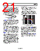
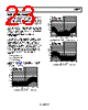
21 / 48 page  Data Sheet AD6677 Rev. C | Page 21 of 48 Input Clock Divider The AD6677 contains an input clock divider with the ability to divide the Nyquist input clock by integer values between 1 and 8. The RF clock input uses an on-chip predivider to divide the clock input by four before it reaches the 1 to 8 divider. This allows higher input frequencies to be achieved on the RF clock input. The divide ratios can be selected using Address 0x09 and Address 0x0B. Address 0x09 sets the RF clock input and Address 0x0B can set the divide ratio of the 1 to 8 divider for both the RF clock input and the Nyquist clock input. For divide ratios other than 1, the duty cycle stabilizer is automatically enabled. RFCLK NYQUIST CLOCK ÷1 TO ÷8 DIVIDER ÷2 OR ÷4 Figure 42. AD6677 Clock Divider Circuit The AD6677 clock divider can be synchronized using the external SYSREF input. Bit 1 and Bit 2 of Address 0x3A allow the clock divider to be resynchronized on every SYSREF signal or only on the first signal after the register is written. A valid SYSREF causes the clock divider to reset to the initial state. This synchronization feature allows multiple devices to align the clock dividers to guarantee simultaneous input sampling. Clock Duty Cycle Typical high speed ADCs use both clock edges to generate a variety of internal timing signals and, as a result, may be sensitive to clock duty cycle. Commonly, a ±5% tolerance is required on the clock duty cycle to maintain dynamic performance characteristics. The AD6677 contains a DCS that retimes the nonsampling (falling) edge, providing an internal clock signal with a nominal 50% duty cycle. This allows the user to provide a wide range of clock input duty cycles without affecting the performance of the AD6677. Jitter on the rising edge of the input clock is still of paramount concern and is not reduced by the DCS. The duty cycle control loop does not function for clock rates of less than 40 MHz nominally. The loop has a time constant associated with it that must be considered when the clock rate can change dynamically. A wait time of 1.5 µs to 5 µs is required after a dynamic clock frequency increase or decrease before the DCS loop is relocked to the input signal. During the time that the loop is not locked, the DCS loop is bypassed, and the internal device timing is dependent on the duty cycle of the input clock signal. In such applications, it may be appropriate to disable the DCS. In all other applications, enabling the DCS circuit is recommended to maximize ac performance. Jitter Considerations High speed, high resolution ADCs are sensitive to the quality of the clock input. The degradation in SNR at a given input frequency (fIN) due to jitter (tJ) can be calculated by SNRHF = −10 log[(2π × fIN × tJRMS)2 + 10 ) 10 / ( LF SNR − ] In the equation, the rms aperture jitter represents the root- mean-square of all jitter sources, which include the clock input, the analog input signal, and the ADC aperture jitter specification. IF undersampling applications are particularly sensitive to jitter, as shown in Figure 43. 50 55 60 65 70 75 80 1 10 100 1000 INPUT FREQUENCY (MHz) 0.05ps 0.2ps 0.5ps 1ps 1.5ps MEASURED Figure 43. SNR vs. Input Frequency and Jitter Treat the clock input as an analog signal in cases where aperture jitter may affect the dynamic range of the AD6677. Separate the power supplies for the clock drivers from the ADC output driver supplies to avoid modulating the clock signal with digital noise. Low jitter, crystal controlled oscillators make the best clock sources. If the clock is generated from another type of source (by gating, dividing, or another method), retime it by using the original clock at the last step. Refer to the Application Note AN-501, Aperture Uncertainty and ADC System Performance, and the Application Note AN-756, Sampled Systems and the Effects of Clock Phase Noise and Jitter, for more information about jitter performance as it relates to ADCs. |
|
Ligação URL |
| ALLDATASHEET é útil para você? [ DONATE ] |
Sobre Alldatasheet | Publicidade | Contato conosco | Privacy Policy | Link para a ficha técnica | roca de Link | Lista de Fabricantes All Rights Reserved©Alldatasheet.com |
| Russian : Alldatasheetru.com | Korean : Alldatasheet.co.kr | Spanish : Alldatasheet.es | French : Alldatasheet.fr | Italian : Alldatasheetit.com Portuguese : Alldatasheetpt.com | Polish : Alldatasheet.pl | Vietnamese : Alldatasheet.vn Indian : Alldatasheet.in | Mexican : Alldatasheet.com.mx | British : Alldatasheet.co.uk | New Zealand : Alldatasheet.co.nz |
|
Family Site : ic2ic.com |
icmetro.com |
 Portuguese ▼
 English
 Chinese
 German
 Japanese
 Russian
 Korean
 Spanish
 French
 Italian
 Portuguese
 Polish
 Vietnamese
 Indian
 Mexican
 British
 New Zealand