|
Os motores de busca de Datasheet de Componentes eletrônicos |
|
|
Os motores de busca de Datasheet de Componentes eletrônicos |
|
AD6677 Folha de dados(PDF) 41 Page - Analog Devices |
|
|
|||||||||||||||||||||||||||||
AD6677 Folha de dados(HTML) 41 Page - Analog Devices |
|
|
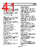
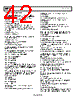
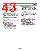
41 / 48 page  Data Sheet AD6677 Rev. C | Page 41 of 48 DC Correction Control (Address 0x40) Bit 7—Reserved Bit 6—Freeze dc correction When Bit 6 is set low, the dc correction is continuously calculated. When Bit 6 is set high, the dc correction is no longer updated to the signal monitor block, which holds the last dc value calculated. Bits[5:2]—DC correction bandwidth select Bits[5:2] set the averaging time of the signal monitor dc correction function. This 4-bit word sets the bandwidth of the correction block, according to the following equation: π × × = − − 2 2 _ _ 14 CLK k f BW Corr DC where: k is the 4-bit value programmed in Bits[5:2] of Address 0x40 (values between 0 and 13 are valid for k; programming 14 or 15 provides the same result as programming 13). fCLK is the AD6677 ADC sample rate in hertz. Bit 1—Enable dc correction Setting this bit high causes the output of the dc measurement block to be summed with the data in the signal path to remove the dc offset from the signal path. Bit 0—Reserved DC Correction Value 0 (Address 0x41) Bits[7:0]—DC correction value LSB[7:0] These bits are the LSBs of the dc correction value. DC Correction Value 1 (Address 0x42) Bits[7:0]—DC correction value MSB[15:8] These bits are the MSBs of the dc correction value. Fast Detect Control (Address 0x45) Bits[7:5]—Reserved Bit 4—FD pin function When this bit is set low, the FD pin functions as the fast detect output. When this pin is set high, the FD pin functions as the overrange indicator. Bit 3—Force FD output enable Setting this bit high forces the FD output pin to the value written to Bit 2 of this register (Address 0x45). This enables the user to force a known value on the FD pin for debugging. Bit 2—Forced FD output value The value written to Bit 2 is forced on the FD output pin when Bit 3 is written high. Bit 1—Reserved Bit 0—Enable fast detect output Setting this bit high enables the output of the upper threshold FD comparator to drive the FD output pin. Fast Detect Upper Threshold (Address 0x47 and Address 0x48) Address 0x48, Bit 7—Reserved Address 0x48, Bits[6:0]—Fast detect upper threshold[14:8] Address 0x47, Bits[7:0]—Fast detect upper threshold[7:0] These registers provide an upper limit threshold. The 15-bit value is compared with the output magnitude from the ADC block. If the ADC magnitude exceeds this threshold value, the FD output pin is set if Bit 0 in Address 0x45 is set. Fast Detect Lower Threshold (Address 0x49 and Address 0x4A) Address 0x4A, Bit 7—Reserved Address 0x4A, Bits[6:0]—Fast detect lower threshold[14:8] Address 0x49, Bits[7:0]—Fast detect lower threshold[7:0] These registers provide a lower limit threshold. The 15-bit value is compared with the output magnitude from the ADC block. If the ADC magnitude is less than this threshold value for the number of cycles programmed in the fast detect dwell time register, the FD output bit is cleared. Fast Detect Dwell Time (Address 0x4B and Address 0x4C) Address 0x4C, Bits[7:0]—Fast detect dwell time[15:8] Address 0x4B, Bits[7:0]—Fast detect dwell time[7:0] These register values set the minimum time in ADC sample clock cycles (after clock divider) that a signal must stay below the lower threshold limit before the FD output bits are cleared. JESD204B Quick Configuration (Address 0x5E) Bits [7:0]—JESD204B quick configuration These bits serve to quickly set up the default JESD204B link parameters for M = 1 and L = 1. JESD204B Link Control 1 (Address 0x5F) Bit 7—Open Bit 6—Serial tail bit enable If this bit is set and the CS bits are not enabled, unused tail bits are padded with a pseudo-random number sequence from a 9-bit LFSR (see JESD204B 5.1.4). Bit 5—JESD204B test sample enable If set, JESD204B test samples are enabled, and the long transport layer test sample sequence (as specified in JESD204B Section 5.1.6.3) sent on all link lanes. Bit 4—Reserved; set to 1 Bits[3:2]—ILAS mode 01 = initial lane alignment sequence enabled. 11 = initial lane alignment sequence always on in test mode; JESD204B data link layer test mode where repeated lane alignment sequence (as specified in JESD204B Section 5.3.3.8.2) is sent on all lanes. Bit 1—Reserved; set to 1 |
|
Ligação URL |
| ALLDATASHEET é útil para você? [ DONATE ] |
Sobre Alldatasheet | Publicidade | Contato conosco | Privacy Policy | Link para a ficha técnica | roca de Link | Lista de Fabricantes All Rights Reserved©Alldatasheet.com |
| Russian : Alldatasheetru.com | Korean : Alldatasheet.co.kr | Spanish : Alldatasheet.es | French : Alldatasheet.fr | Italian : Alldatasheetit.com Portuguese : Alldatasheetpt.com | Polish : Alldatasheet.pl | Vietnamese : Alldatasheet.vn Indian : Alldatasheet.in | Mexican : Alldatasheet.com.mx | British : Alldatasheet.co.uk | New Zealand : Alldatasheet.co.nz |
|
Family Site : ic2ic.com |
icmetro.com |
 Portuguese ▼
 English
 Chinese
 German
 Japanese
 Russian
 Korean
 Spanish
 French
 Italian
 Portuguese
 Polish
 Vietnamese
 Indian
 Mexican
 British
 New Zealand