|
Os motores de busca de Datasheet de Componentes eletrônicos |
|
|
Os motores de busca de Datasheet de Componentes eletrônicos |
|
AD6677 Folha de dados(PDF) 20 Page - Analog Devices |
|
|
|||||||||||||||||||||||||||||
AD6677 Folha de dados(HTML) 20 Page - Analog Devices |
|
|
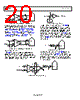
20 / 48 page  AD6677 Data Sheet Rev. C | Page 20 of 48 100Ω 0.1µF 0.1µF 0.1µF 0.1µF 240Ω 240Ω PECL DRIVER 50kΩ 50kΩ CLK– CLK+ CLOCK INPUT CLOCK INPUT AD95xx ADC Figure 37. Differential PECL Sample Clock (Up to 625 MHz) Analog Devices also offers LVDS clock drivers with excellent jitter performance. Figure 38 shows a typical circuit. This illustrates using LVDS drivers such as the AD9510, AD9511, AD9512, AD9513, AD9514, AD9515, the AD9516-0 through AD9516-5 device family, the AD9517-0 through AD9517-4 device family, the AD9518-0 through AD9518-4 device family, the AD9520-0 through AD9520-5 device family, the AD9522-0 through AD9522-5 device family, AD9523, and AD9524. 100Ω 0.1µF 0.1µF 0.1µF 0.1µF 50kΩ 50kΩ CLK– CLK+ CLOCK INPUT CLOCK INPUT AD95xx LVDS DRIVER ADC Figure 38. Differential LVDS Sample Clock (Up to 625 MHz) RF Clock Input Options The AD6677 RF clock input supports a single-ended clock between 500 MHz to 1.5 GHz. The equivalent RF clock input circuit is shown in Figure 39. The input is self biased to 0.9 V and is typically ac-coupled. The input has a typical input impedance of 10 kΩ in parallel with 0.5 pF at the RFCLK pin. BIAS CONTROL 10kΩ RFCLK INTERNAL CLOCK DRIVER 0.5pF Figure 39. Equivalent RF Clock Input Circuit It is recommended that the RF clock input of the AD6677 be driven with a PECL or sine wave signal with a minimum signal amplitude of 600 mV p-p. Regardless of the type of signal used, clock source jitter is of the most concern, as described in the Jitter Considerations section. Figure 40 shows the preferred method of clocking when using the RF clock input on the AD6677. Due to the high frequency nature of the signal, it is recommended to use a 50 Ω transmission line to route the clock signal to the RF clock input of the AD6677 and terminate the transmission line close to the RF clock input. RFCLK ADC 50Ω Tx LINE RF CLOCK INPUT 0.1µF 50Ω Figure 40. Typical RF Clock Input Circuit Figure 41 shows the RF clock input of the AD6677 being driven from the LVPECL outputs of the AD9515. The differential LVPECL output signal from the AD9515 is converted to a single- ended signal using an RF balun or RF transformer. The RF balun configuration is recommended for clock frequencies associated with the RF clock input. 0.1µF 0.1µF 0.1µF 0.1µF LVPECL DRIVER AD9515 127Ω VDD 82.5Ω 127Ω 82.5Ω CLOCK INPUT CLOCK INPUT RFCLK ADC 50Ω Tx LINE 0.1µF 50Ω Figure 41. Differential PECL RF Clock Input Circuit |
|
Ligação URL |
| ALLDATASHEET é útil para você? [ DONATE ] |
Sobre Alldatasheet | Publicidade | Contato conosco | Privacy Policy | Link para a ficha técnica | roca de Link | Lista de Fabricantes All Rights Reserved©Alldatasheet.com |
| Russian : Alldatasheetru.com | Korean : Alldatasheet.co.kr | Spanish : Alldatasheet.es | French : Alldatasheet.fr | Italian : Alldatasheetit.com Portuguese : Alldatasheetpt.com | Polish : Alldatasheet.pl | Vietnamese : Alldatasheet.vn Indian : Alldatasheet.in | Mexican : Alldatasheet.com.mx | British : Alldatasheet.co.uk | New Zealand : Alldatasheet.co.nz |
|
Family Site : ic2ic.com |
icmetro.com |
 Portuguese ▼
 English
 Chinese
 German
 Japanese
 Russian
 Korean
 Spanish
 French
 Italian
 Portuguese
 Polish
 Vietnamese
 Indian
 Mexican
 British
 New Zealand