|
Os motores de busca de Datasheet de Componentes eletrônicos |
|
|
Os motores de busca de Datasheet de Componentes eletrônicos |
|
AD6677 Folha de dados(PDF) 36 Page - Analog Devices |
|
|
|||||||||||||||||||||||||||||
AD6677 Folha de dados(HTML) 36 Page - Analog Devices |
|
|
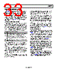
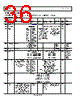
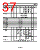
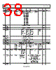
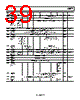
36 / 48 page  AD6677 Data Sheet Rev. C | Page 36 of 48 MEMORY MAP REGISTER TABLE All address and bit locations that are not included in Table 17 are not currently supported for this device. Table 17. Memory Map Registers Reg Addr (Hex) Reg Addr Name Bit 7 (MSB) Bit 6 Bit 5 Bit 4 Bit 3 Bit 2 Bit 1 Bit 0 (LSB) Default Notes 0x00 SPI port configuration 0 LSB first Soft reset 1 1 Soft reset LSB first 0 0x18 0x01 Chip ID AD6677 8-bit Chip ID is 0xC4 0xC4 Read only 0x02 Chip grade Speed grade: 00 = 250 MSPS Reserved for chip die revision currently 0x0 0x00 0x08 PDWN modes External PDWN mode: 0 = PDWN is full power- down, 1 = PDWN puts device in standby JESD204B standby mode (when external PDWN is used): 0 = JESD204B core is unaffected, 1 = JESD204B core is powered down except for PLL JESD204B power modes: 00 = normal mode (power-up); 01 = power-down mode, PLL off, serializer off, clocks stopped, digital held in reset; 10 = standby mode: PLL on, serializer off, clocks stopped, digital circuitry held in reset ADC power modes: 00 = normal mode (power-up), 01 = power-down mode, 10 = standby mode, does not affect JESD204B digital circuitry 0x00 0x09 Global clock Reserved Clock selection: 00 = Nyquist clock, 01 = RF clock divide by 2, 10 = RF clock divide by 4, 11 = clock off Clock duty cycle stabilizer enable 0x01 DCS enabled if clock divider enabled 0x0A PLL status PLL locked status JESD204B link is ready Read only 0x0B Clock divider Clock divide phase relative to the encode clock: 0x0 = 0 input clock cycles delayed, 0x1 = 1 input clock cycles delayed, 0x2 = 2 input clock cycles delayed, … 0x7 = 7 input clock cycles delayed Clock divider ratio relative to the encode clock: 0x00 = divide by 1, 0x01 = divide by 2, 0x02 = divide by 3, … 0x07 = divide by 8 0x00 Clock divide values other than 0x00 automatically cause the DCS to become active 0x0D Test mode User test mode cycle: 00 = repeat pattern (user pattern 1, 2, 3, 4, 1, 2, 3, 4, 1, …); 10 = single pattern (user pattern 1, 2, 3, 4, then all zeros) Long pseudo- random number generator reset: 0 = long PRN enabled, 1 = long PRN held in reset Short pseudo- random number generator reset: 0 = short PRN enabled, 1 = short PRN held in reset Data output test generation mode: 0000 = off (normal mode), 0001 = midscale short, 0010 = positive full scale, 0011 = negative full scale, 0100 = alternating checkerboard, 0101 = PN sequence long, 0110 = PN sequence short, 0111 = 1/0 word toggle, 1000 = user test mode (use with Address 0x0D, Bits[7:6] and user pattern 1, 2, 3, 4), 1001 to 1110 = unused, 1111 = ramp output 0x00 0x10 Customer offset Offset adjust in LSBs from +31 to −32 (twos complement format): 01 1111 = adjust output by +31, 01 1110 = adjust output by +30, … 00 0001 = adjust output by +1, 00 0000 = adjust output by 0 (default), … 10 0001 = adjust output by −31, 10 0000 = adjust output by −32 0x00 0x14 Output mode JESD204B CS bits assignment (in conjunction with Address 0x72): 000 = {overrange||underrange, valid}, 001 = {overrange, underrange}, 010 = {overrange||underrange, blank}, 011 = {blank, valid}, 100 = {blank, blank}, 101 = {underrange, overrange}, 110 = {valid, overange||underrange}, 111 = {valid, blank} ADC output disable ADC data invert: 0 = normal (default), 1 = inverted Data format select (DFS): 00 = offset binary, 01 = twos complement 0x01 |
|
Ligação URL |
| ALLDATASHEET é útil para você? [ DONATE ] |
Sobre Alldatasheet | Publicidade | Contato conosco | Privacy Policy | Link para a ficha técnica | roca de Link | Lista de Fabricantes All Rights Reserved©Alldatasheet.com |
| Russian : Alldatasheetru.com | Korean : Alldatasheet.co.kr | Spanish : Alldatasheet.es | French : Alldatasheet.fr | Italian : Alldatasheetit.com Portuguese : Alldatasheetpt.com | Polish : Alldatasheet.pl | Vietnamese : Alldatasheet.vn Indian : Alldatasheet.in | Mexican : Alldatasheet.com.mx | British : Alldatasheet.co.uk | New Zealand : Alldatasheet.co.nz |
|
Family Site : ic2ic.com |
icmetro.com |
 Portuguese ▼
 English
 Chinese
 German
 Japanese
 Russian
 Korean
 Spanish
 French
 Italian
 Portuguese
 Polish
 Vietnamese
 Indian
 Mexican
 British
 New Zealand