 |
Os motores de busca de Datasheet de Componentes eletrônicos |
|
|
Os motores de busca de Datasheet de Componentes eletrônicos |
|
The question interval is too short.
Please try again in a few seconds.

Hello, Please ask a question about AD6677 Datasheet
# Example questions:
➢ What is the maximum input resistance (ac-coupled) for the rf clock input (rfclk)?
➢ What are the three logic compliance options for the rf clock input (rfclk)?
➢ What is the typical differential output voltage (vod) for the digital outputs serdout0+/serdout0−?
| Part No. | AD6677 |
| Manufacturer | AD |
| Size | 1Mb |
| Pages | 48 pages |
| Description | 80 MHz Bandwidth, IF Receiver |


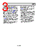
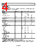

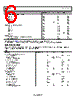
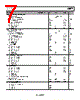


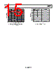
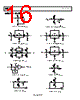
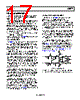
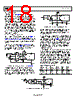
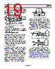
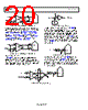
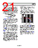
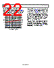
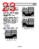
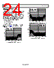
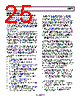
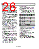
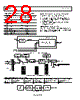
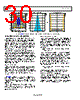
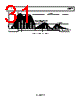
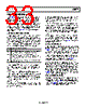
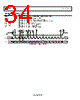
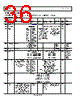
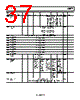
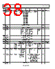
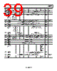
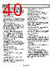
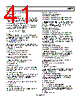
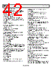

Okay, I'm going to summarize the key information from the provided AD6677 datasheet excerpts. This will be organized into sections: Overview, Analog Inputs, Digital Inputs/Outputs and General Characteristics.
1. Overview:
️· The AD6677 is a high-speed Analog-to-Digital Converter (ADC).
️· It appears to be designed for applications requiring precise sampling and synchronization.
2. Analog Inputs:
️· Input Voltage Range: Specific input voltage ranges are detailed for different signals and digital ports. These are critical for operating the ADC correctly.
️· Differential Inputs: Many inputs (e.g., CLK+, CLK-, SYNCINB+, SYNCINB-, SYSREF+, SYSREF-) are differential, requiring careful attention to common-mode voltages and signal integrity.
️· Input Resistances: Input resistances (in kOhms) are listed for various analog and digital input signals. This is useful for impedance matching and circuit design.
️· Input Capacitance: Capacitance values are given for different inputs.
3. Digital Inputs/Outputs:
️· Logic Levels: The datasheet defines high and low voltage levels for digital inputs and outputs. This dictates the required logic levels for the external circuitry.
️· Logic Compliance: The ADC supports various logic standards: CMOS, LVDS, and LVPECL.
️· Digital Output Voltage (VOD): For the digital outputs, a target output voltage (VOD) is specified with a value of 400mV.
️· SDIO port: The SDIO port has unique characteristic than others.
️· Digital Outputs (SERDOUT0+/SERDOUT0-): These outputs have specific characteristics and target voltage levels.
️· Digital Output High Voltage (VOH): Depending on the output drive current, the high-level output voltage (VOH) changes.
4. General Characteristics:
️· Clock Rates: The ADC supports high clock rates for differential and RF clock inputs (up to 500 MHz and 1500 MHz, respectively).
️· Internal Biases: Many inputs have internal common-mode biases, reducing the need for external biasing circuits.
️· Input Resistance: Many inputs have defined input resistance.
️· Input Capacitance: Capacitance values are given for different inputs.
️· Input Voltage Range: Input voltage ranges for various signal and digital ports.
Important Notes & Limitations of Summary:
️· Incomplete Document: This is an *excerpt* from a datasheet. A full datasheet would provide far more detail, including ADC resolution, sampling rate, power consumption, and timing diagrams.
️· Specialized Information: The information contained is highly specialized, relevant to electrical engineers and circuit designers working with ADCs.
️· Context is Key: The specific values given (voltages, resistances, capacitances) are only meaningful within the context of the AD6677's overall architecture and operating conditions.
️· Careful Review: Any circuit design involving the AD6677 should be based on a full review of the complete datasheet and associated application notes.
1. Overview:
️· The AD6677 is a high-speed Analog-to-Digital Converter (ADC).
️· It appears to be designed for applications requiring precise sampling and synchronization.
2. Analog Inputs:
️· Input Voltage Range: Specific input voltage ranges are detailed for different signals and digital ports. These are critical for operating the ADC correctly.
️· Differential Inputs: Many inputs (e.g., CLK+, CLK-, SYNCINB+, SYNCINB-, SYSREF+, SYSREF-) are differential, requiring careful attention to common-mode voltages and signal integrity.
️· Input Resistances: Input resistances (in kOhms) are listed for various analog and digital input signals. This is useful for impedance matching and circuit design.
️· Input Capacitance: Capacitance values are given for different inputs.
3. Digital Inputs/Outputs:
️· Logic Levels: The datasheet defines high and low voltage levels for digital inputs and outputs. This dictates the required logic levels for the external circuitry.
️· Logic Compliance: The ADC supports various logic standards: CMOS, LVDS, and LVPECL.
️· Digital Output Voltage (VOD): For the digital outputs, a target output voltage (VOD) is specified with a value of 400mV.
️· SDIO port: The SDIO port has unique characteristic than others.
️· Digital Outputs (SERDOUT0+/SERDOUT0-): These outputs have specific characteristics and target voltage levels.
️· Digital Output High Voltage (VOH): Depending on the output drive current, the high-level output voltage (VOH) changes.
4. General Characteristics:
️· Clock Rates: The ADC supports high clock rates for differential and RF clock inputs (up to 500 MHz and 1500 MHz, respectively).
️· Internal Biases: Many inputs have internal common-mode biases, reducing the need for external biasing circuits.
️· Input Resistance: Many inputs have defined input resistance.
️· Input Capacitance: Capacitance values are given for different inputs.
️· Input Voltage Range: Input voltage ranges for various signal and digital ports.
Important Notes & Limitations of Summary:
️· Incomplete Document: This is an *excerpt* from a datasheet. A full datasheet would provide far more detail, including ADC resolution, sampling rate, power consumption, and timing diagrams.
️· Specialized Information: The information contained is highly specialized, relevant to electrical engineers and circuit designers working with ADCs.
️· Context is Key: The specific values given (voltages, resistances, capacitances) are only meaningful within the context of the AD6677's overall architecture and operating conditions.
️· Careful Review: Any circuit design involving the AD6677 should be based on a full review of the complete datasheet and associated application notes.
| Part No. | AD6677 |
| Manufacturer | AD |
| Size | 1Mb |
| Pages | 48 pages |
| Description | 80 MHz Bandwidth, IF Receiver |
| ALLDATASHEET é útil para você? [ DONATE ] |
Sobre Alldatasheet | Publicidade | Contato conosco | Privacy Policy | Link para a ficha técnica | roca de Link | Lista de Fabricantes All Rights Reserved©Alldatasheet.com |
| Russian : Alldatasheetru.com | Korean : Alldatasheet.co.kr | Spanish : Alldatasheet.es | French : Alldatasheet.fr | Italian : Alldatasheetit.com Portuguese : Alldatasheetpt.com | Polish : Alldatasheet.pl | Vietnamese : Alldatasheet.vn Indian : Alldatasheet.in | Mexican : Alldatasheet.com.mx | British : Alldatasheet.co.uk | New Zealand : Alldatasheet.co.nz |
|
Family Site : ic2ic.com |
icmetro.com |
 Portuguese ▼
  English
 Chinese
 German
 Japanese
 Russian
 Korean
 Spanish
 French
 Italian
 Polish
 Vietnamese
 Indian
 Mexican
 British
 New Zealand