|
Os motores de busca de Datasheet de Componentes eletrônicos |
|
|
Os motores de busca de Datasheet de Componentes eletrônicos |
|
ADIN2111BCPZ-R7 Folha de dados(PDF) 39 Page - Analog Devices |
|
|
|||||||||||||||||||||||||||||
ADIN2111BCPZ-R7 Folha de dados(HTML) 39 Page - Analog Devices |
|
|
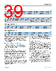
39 / 129 page  Data Sheet ADIN2111 SWITCH SPI analog.com Rev. A | 39 of 129 Table 33. Control Write Transaction with CRC MSB LSB D102 D101 D101 D100 to D89 D88 to D80 D79 to D48 D47 to D40 D39 to D8 D7 to D0 SDI 1 0 R/W ADDR[12:0] CRC[7:0] DATA0[31:0] CRC[7:0] DATA1[31:0] CRC[7:0] Table 34. Control Read Transaction with CRC MSB LSB D110 D109 D108 D107 to D96 D95 to D88 D87 to D80 D79 to D48 D47 to D40 D39 to D8 D7 to D0 SDI 1 0 R/W ADDR[12:0] CRC[7:0] TA[7:0] 0 0 0 0 SDO DATA0[31:0] CRC[7:0] DATA1[31:0] CRC[7:0] Table 35. Data Write Transaction with CRC MSB LSB D86 D85 D84 D83 to D71 D71 to D64 D63 to D32 D31 to D0 SDI 1 0 R/W ADDR[12:0] CRC[7:0] DATA0[31:0] DATA1[31:0] Table 36. Data Read Transaction with CRC MSB LSB D94 D93 D92 D91 to D80 D79 to D72 D71 to D64 D63 to D32 D31 to 0 SDI 1 0 R/W ADDR[12:0] CRC[7:0] TA[7:0] 0 0 SDO DATA0[31:0] DATA1[31:0] The generic SPI protocol is half duplex. Therefore, it is not possible to write frame data into the MAC_TX register and read from the MAC_RX register at the same time. Because of this, the SPI SCLK frequency must be 25 MHz to achieve full duplex transmissions on Ethernet at 10 Mbps. MAC Frame: Transmit and Receive The 2-byte frame header shown in Table 37 is appended to all transmitted and received frames. This frame header always pre- cedes the frame data (see Figure 22). Time Stamp Capture On receive, if TIME_STAMP_PRESENT is asserted, an additional 4-byte or 8-byte time stamp is provided after the 2-byte header in Table 37 and before the data frame. This time stamp can then be stored or discarded by software when reading the receive FIFO. On transmit, if EGRESS_CAPTURE is set other than 00, the ADIN2111 captures the time stamp of the transmitted frame into the respective TTSCxH and TTSCxL registers for Port 1, and P2_TTSCxH and P2_TTSCxL for Port 2. To enable the time stamp capture signal pin, enable the P1_LED_0 or TEST_1 pins to be muxed as the time stamp input pin using the DIGIO_TSCAPT_PINMUX bits field in the Pin Mux Configuration 1 register (DIGIO_PINMUX). The time stamp counter can be enabled by setting TS_EN (TS_CFG register) to 1 and setting FTSE (CONFIG0 register) to 1. Time Stamp Timer Output The ADIN2111 supports a TS_TIMER output signal. TS_TIMER can be started at a defined time relative to the nanoseconds counter. The TS_TIMER counter start time register (TS_TIMER_START) is used to set the start time. TS_TIMER then toggles based on the high and low times configured in high period for the TS_TIMER register (TS_TIMER_HI) and low period for the TS_TIMER register (TS_TIMER_LO). Use the following sequence to enable the TS_TIMER output: 1. Configure the P1_LED_0 pin to the TS_TIMER function using the LED control register (LED_CNTRL). 2. To change the default value of the TS_TIMER from 0 to 1, write 1 to TS_TIMER_DEF in the timer configuration register (TS_CFG). TS_TIMER immediately toggles from 0 to 1. 3. Write to the TS_TIMER_HI and TS_TIMER_LO bits to set the required high time and low time for the TS_TIMER output. 4. Configure the quantization error correction register (TS_TIM- ER_QE_CORR) to set the required quantization error correc- tion. |
|
Ligação URL |
| ALLDATASHEET é útil para você? [ DONATE ] |
Sobre Alldatasheet | Publicidade | Contato conosco | Privacy Policy | Link para a ficha técnica | roca de Link | Lista de Fabricantes All Rights Reserved©Alldatasheet.com |
| Russian : Alldatasheetru.com | Korean : Alldatasheet.co.kr | Spanish : Alldatasheet.es | French : Alldatasheet.fr | Italian : Alldatasheetit.com Portuguese : Alldatasheetpt.com | Polish : Alldatasheet.pl | Vietnamese : Alldatasheet.vn Indian : Alldatasheet.in | Mexican : Alldatasheet.com.mx | British : Alldatasheet.co.uk | New Zealand : Alldatasheet.co.nz |
|
Family Site : ic2ic.com |
icmetro.com |
 Portuguese ▼
 English
 Chinese
 German
 Japanese
 Russian
 Korean
 Spanish
 French
 Italian
 Portuguese
 Polish
 Vietnamese
 Indian
 Mexican
 British
 New Zealand