|
Os motores de busca de Datasheet de Componentes eletrônicos |
|
|
Os motores de busca de Datasheet de Componentes eletrônicos |
|
ADMV1455BBCZ-R7 Folha de dados(PDF) 66 Page - Analog Devices |
|
|
|||||||||||||||||||||||||||||
ADMV1455BBCZ-R7 Folha de dados(HTML) 66 Page - Analog Devices |
|
|
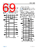
66 / 141 page  Data Sheet ADMV1455 THEORY OF OPERATION analog.com Rev. 0 | 66 of 141 SPI The ADMV1455 utilizes the SPI for communication to configure the chip settings. The SPI can be implemented in either 3-wire or 4-wire configurations, supports 1.8V logic levels, and SCLK frequencies up to 125MHz. The SPI consists of digital inputs and outputs. CHIP_ADD0, CHIP_ADD1, SCLK, and CS are the digital inputs. SDIO is bidirec- tional and can be an input or output, depending upon the type of SPI operation being performed, and SDO is a digital output that remains in a high impedance state unless a read operation is being performed. CS is an active low digital input and must be asserted low during a SPI instruction. Be sure to deasserted CS at the end of a SPI instruction. The chip address inputs, CHIP_ADD0 and CHIP_ADD1, can be used in multichip systems to assign an address to a particular chip. This feature allows up to four chips to share SCLK, SDIO, SDO, and CS connections. To set a chip address input to 0, ground the ball or add a 0Ω pull-down resistor. To set a chip address input to 1, leave it floating, and the internal 15kΩ resistor will set it to a logic level high. The assigned chip address modifies the SPI Communications Frame Bits[21:20]. For single SPI instructions, the communications frame is 24-bits wide and consists of a 16-bit header and 8 bits of data. The header contains a R/W bit, a broadcast (BR) bit, two chip address bits, and 12 register address bits. Both the header and data are organized MSB first and must be shifted in on SDIO with the chip sampling the logic level on the rising edge of SCLK. See Figure 166 for the SPI communications frame. Set the R/W bit to 0 for a write operation and set the R/W to 1 for a read operation. Set the BR bit to 0 for single chip SPI instructions and set this bit to 1 to have all chips, regardless of their chip address, respond to a SPI instruction. For read operations, the BR bit must only be set to 0. For a read operation when using a 3-wire SPI, the SDIO changes from an input to an output after the last header SCLK rising edge. The data is then shifted out on SDIO, with the logic level changing on the falling edge of SCLK, so that it can be sampled on the next rising edge of SCLK. When CS is deasserted, SDIO changes back to a digital input. For a read operation when using a 4-wire SPI, the SDO transitions from a high impedance state to an active output, after the last header SCLK rising edge. The data is then shifted out on SDO, with the logic level changing on the falling edge of SCLK, so that it can be sampled on the next rising edge of SCLK. When CS is deasserted, SDO returns to a high impedance state. The ADMV1455 supports SPI streaming that minimizes the SPI instruction time. During a SPI streaming instruction, CS is asserted low, a single 16-bit header instruction is given, followed by multiple bytes of data, and then CS is deasserted to end the instruction. Sequential register addresses are assumed in ascending or de- scending order based on how Register 0x000, Bit 5 and Bit 2 are set. Note that the default order is descending addresses. If CS is deasserted during any header portion of a SPI instruction, the operation is ignored. If CS is deasserted during a data portion of a SPI instruction, then that data is ignored. For SPI streaming operations, any complete bytes (8 bits) of data are accepted by the chip, but a partial byte is ignored. See the Timing Diagrams Overview section, the Power-Up and Apply the Digital Inputs section, the Initialization SPI Instructions section, the Chip Enable and Operation section, the Chip Disable and Reset section, and the Chip Disable and Power-Down section for additional timing information and refer to the ADI-SPI, Serial Control Interface Standard (Rev 1.0) for more information on SPI and communications protocol. Figure 166. Single SPI Frame Timing Diagram |
|
Ligação URL |
| ALLDATASHEET é útil para você? [ DONATE ] |
Sobre Alldatasheet | Publicidade | Contato conosco | Privacy Policy | Link para a ficha técnica | roca de Link | Lista de Fabricantes All Rights Reserved©Alldatasheet.com |
| Russian : Alldatasheetru.com | Korean : Alldatasheet.co.kr | Spanish : Alldatasheet.es | French : Alldatasheet.fr | Italian : Alldatasheetit.com Portuguese : Alldatasheetpt.com | Polish : Alldatasheet.pl | Vietnamese : Alldatasheet.vn Indian : Alldatasheet.in | Mexican : Alldatasheet.com.mx | British : Alldatasheet.co.uk | New Zealand : Alldatasheet.co.nz |
|
Family Site : ic2ic.com |
icmetro.com |
 Portuguese ▼
 English
 Chinese
 German
 Japanese
 Russian
 Korean
 Spanish
 French
 Italian
 Portuguese
 Polish
 Vietnamese
 Indian
 Mexican
 British
 New Zealand