|
Os motores de busca de Datasheet de Componentes eletrônicos |
|
|
Os motores de busca de Datasheet de Componentes eletrônicos |
|
CC1010-RTY1 Folha de dados(PDF) 68 Page - Texas Instruments |
|
|
|
|||||||||||||||||||||||||||||
CC1010-RTY1 Folha de dados(HTML) 68 Page - Texas Instruments |
|
|
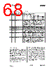
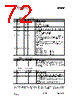
68 / 152 page  CC1010 SWRS047 Page 68 of 152 SCON1 (0xC0) - Serial Port 1 Control Register Bit Name R/W Reset value Description 7 SM0_1 R/W 0 6 SM1_1 R/W 0 Serial Port 1 mode bits, decoded as: SM0_1 SM1_1 Mode 0 0 0 (Synchronous half duplex) 0 1 1 (Asynchronous full duplex, start + stop bit) 1 0 2 (Asynchronous full duplex, start + stop bit, 9th data bit) 1 1 3 (Asynchronous full duplex, start + stop bit, 9th data bit) 5 SM2_1 R/W 0 Multiprocessor communication enable. In modes 2 and 3 SM2_1 = 1 enables the multiprocessor communication feature: In mode 2 or 3 RI_1 will not be activated if the received 9th bit is 0. If SM2_1 = 1 in mode 1 RI_1 will only be activated if a valid stop bit is received. In mode 0 SM2_1 establishes the baud rate: when SM2_1 = 0 the baud rate is clk / 12; when SM2_1= 1 the baud rate is clk / 4. 4 REN_1 R/W 0 Receive enable. When REN_1 = 1 reception is enabled. 3 TB8_1 R/W 0 Defines the state of the 9th data bit transmitted in modes 2 and 3. 2 RB8_1 R/W 0 In modes 2 and 3 RB8_1 indicates the state of the 9th bit received. In mode 1 RB8_1 indicates the state of the received stop bit. In mode 0 RB8_1 is not used. 1 TI_1 R/W 0 Transmit interrupt flag. Indicates that the transmit data word has been shifted out. In mode 0 TI_1 is set at the end of the 8th data bit. In all other modes TI_1 is set when the stop bit is placed on the TXD1 pin. TI_1 must be cleared by the software. 0 RI_1 R/W 0 Receive interrupt flag. Indicates that a serial data word has been received. In mode 0 RI_1 is set at the end of the 8th data bit. In mode 1 RI_1 is set after the last sample of the incoming stop bit, subject to the state of SM2_1. In modes 2 and 3 RI_1 is set at the end of the last sample of RB8_1. RI_1 must be cleared by the software. 16.7.1 MODE 0 Serial mode 0 provides synchronous, half- duplex serial communication. For serial port 0, pin RXD0 (P3.0) is used for data input and output while TXD0 (P3.1) provides the bit clock for both transmit and receive. For serial port 1 the corresponding pins are RXD1 (P2.0) and TXD1 (P2.1). The serial mode 0 baud rate is set by SCON0.SM2_0 / SCON1.SM2_1. If this bit is cleared, the baud rate is the system clock divided by 4. If the bit is set, the system clock is divided by 12. Data transmission begins when an instruction writes to the SBUF0 (or SBUF1) register. The serial port shifts the data byte out, LSB first, at the selected baud rate. Data reception starts when SCON0.REN_0 / SCON1.REN_1 is set and the receive interrupt flag SCON0.RI_0 / SCON1.RI_1 is cleared. The bit clock is activated and the UART shifts data in on each rising edge of the bit clock, until 8 bits have been received. Immediately after the 8th bit is shifted in, the receive interrupt flag is set and reception stops until the software clears the flag. |
|
Ligação URL |
| ALLDATASHEET é útil para você? [ DONATE ] |
Sobre Alldatasheet | Publicidade | Contato conosco | Privacy Policy | Link para a ficha técnica | roca de Link | Lista de Fabricantes All Rights Reserved©Alldatasheet.com |
| Russian : Alldatasheetru.com | Korean : Alldatasheet.co.kr | Spanish : Alldatasheet.es | French : Alldatasheet.fr | Italian : Alldatasheetit.com Portuguese : Alldatasheetpt.com | Polish : Alldatasheet.pl | Vietnamese : Alldatasheet.vn Indian : Alldatasheet.in | Mexican : Alldatasheet.com.mx | British : Alldatasheet.co.uk | New Zealand : Alldatasheet.co.nz |
|
Family Site : ic2ic.com |
icmetro.com |
 Portuguese ▼
 English
 Chinese
 German
 Japanese
 Russian
 Korean
 Spanish
 French
 Italian
 Portuguese
 Polish
 Vietnamese
 Indian
 Mexican
 British
 New Zealand