|
Os motores de busca de Datasheet de Componentes eletrônicos |
|
|
Os motores de busca de Datasheet de Componentes eletrônicos |
|
BMP280 Folha de dados(PDF) 30 Page - Bosch Sensortec GmbH |
|
|
|||||||||||||||||||||||||||||
BMP280 Folha de dados(HTML) 30 Page - Bosch Sensortec GmbH |
|
|
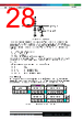
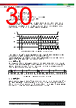
30 / 49 page  Bosch Sensortec | BMP280 Data sheet 30 | 49 Modifications reserved | Data subject to change without notice Document number: BST-BMP280-DS001-26 Revision_1.26_102021 The SPI interface uses the following pins: • CSB: chip select, active low • SCK: serial clock • SDI: serial data input; data input/output in 3-wire mode • SDO: serial data output; hi-Z in 3-wire mode Refer to chapter 6 for connection instructions. CSB is active low and has an integrated pull-up resistor. Data on SDI is latched by the device at SCK rising edge and SDO is changed at SCK falling edge. Communication starts when CSB goes to low and stops when CSB goes to high; during these transitions on CSB, SCK must be stable. The SPI protocol is shown in Figure 9. For timing details, please review Table 28 . CSB SCK SDI RW AD6 AD5 AD4 AD3 AD2 AD1 AD0 DI5 DI4 DI3 DI2 DI1 DI0 DI7 DI6 SDO DO5 DO4 DO3 DO2 DO1 DO0 DO7 DO6 tri-state Figure 9: SPI protocol (shown for mode ‘11’ in 4-wire configuration) In SPI mode, only 7 bits of the register addresses are used; the MSB of register address is not used and replaced by a read/write bit (RW = ‘0’ for write and RW = ‘1’ for read). Example: address 0xF7 is accessed by using SPI register address 0x77. For write access, the byte 0x77 is transferred, for read access, the byte 0xF7 is transferred. 5.3.1 SPI write Writing is done by lowering CSB and sending pairs control bytes and register data. The control bytes consist of the SPI register address (= full register address without bit 7) and the write command (bit7 = RW = ‘0’). Several pairs can be written without raising CSB. The transaction is ended by a raising CSB. The SPI write protocol is depicted in Figure 10. Start RW RW Stop 0 1 1 1 0 1 0 0 bit7 bit6 bit5 bit4 bit3 bit2 bit1 bit0 0 1 1 1 0 1 0 1 bit7 bit6 bit5 bit4 bit3 bit2 bit1 bit0 Control byte CSB = 1 Data byte Register address (F5h) Data register - adress F5h Register address (F4h) CSB = 0 Control byte Data byte Data register - address F4h Figure 10: SPI multiple byte write (not auto-incremented) 5.3.2 SPI read Reading is done by lowering CSB and first sending one control byte. The control bytes consist of the SPI register address (= full register address without bit 7) and the read command (bit 7 = RW = ‘1’). After writing the control byte, data is sent out of the SDO pin (SDI in 3-wire mode); the register address is automatically incremented. The SPI read protocol is shown in Figure 11. |
|
Ligação URL |
| ALLDATASHEET é útil para você? [ DONATE ] |
Sobre Alldatasheet | Publicidade | Contato conosco | Privacy Policy | Link para a ficha técnica | roca de Link | Lista de Fabricantes All Rights Reserved©Alldatasheet.com |
| Russian : Alldatasheetru.com | Korean : Alldatasheet.co.kr | Spanish : Alldatasheet.es | French : Alldatasheet.fr | Italian : Alldatasheetit.com Portuguese : Alldatasheetpt.com | Polish : Alldatasheet.pl | Vietnamese : Alldatasheet.vn Indian : Alldatasheet.in | Mexican : Alldatasheet.com.mx | British : Alldatasheet.co.uk | New Zealand : Alldatasheet.co.nz |
|
Family Site : ic2ic.com |
icmetro.com |
 Portuguese ▼
 English
 Chinese
 German
 Japanese
 Russian
 Korean
 Spanish
 French
 Italian
 Portuguese
 Polish
 Vietnamese
 Indian
 Mexican
 British
 New Zealand