|
Os motores de busca de Datasheet de Componentes eletrônicos |
|
|
Os motores de busca de Datasheet de Componentes eletrônicos |
|
ATXP032 Folha de dados(PDF) 9 Page - Dialog Semiconductor |
|
|
|||||||||||||||||||||||||||||
ATXP032 Folha de dados(HTML) 9 Page - Dialog Semiconductor |
|
|
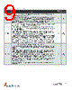
9 / 113 page  7 ATXP032 DS-ATXP032–114I–4-2020 SCK SERIAL CLOCK: This pin is used to provide a clock to the device and is used to control the flow of data to and from the device. In Single Data Rate (SDR) modes, command, address, and input data present on the I/O pins are always latched in on the rising edge of SCK, while output data on the I/O pins is always clocked out on the falling edge of SCK. In the Double Data Rate (DDR) modes, address and input data present on the I/O pins data are latched on both clock edges. For more accurate operation at high speeds, SCK is returned as DS synchronous to output data. - Input SI (I/O 0) SERIAL INPUT: In SPI mode, the SI pin is used to shift data into the device. The SI pin is used for all data input including command and address sequences. In SDR modes, command, address, and input data present on the SI pin is always latched in on the rising edge of SCK. In the DDR modes, address and input data present on the SI pin is latched on both edges of SCK. In octal mode, the SI Pin becomes an I/O pin (I/O 0) in conjunction with other pins. In SDR modes this allows eight bits of command, address, or input data on I/O 7-0 to be clocked in on the rising edge of SCK, or eight bits clocked out on the falling edge of SCK. In Double Data Rate (DDR) mode this allows eight bits of address or input data on I/O7-0 to be clocked in on every edge of SCK, or eight bits clocked out on every edge of SCK. Commands are clocked on the rising edge of SCK, requiring a whole clock cycle also in the DDR modes. To maintain consistency with the SPI nomenclature, the SI (I/O 0) pin is referenced as the SI pin, unless specifically addressing the multi-I/O modes, in which case it is referenced as I/O0. Data present on the SI pin is ignored whenever the device is deselected (CS is deasserted). - Input/ Output SO (I/O 1) SERIAL OUTPUT: The SO pin is used to shift data out from the device. In the Single Data Rate (SDR) mode, data on the SO pin is always clocked out on the falling edge of SCK. In the Double Data Rate (DDR) mode, data on the SO pin is clocked out on both edges of SCK. In octal mode, the SO Pin becomes an I/O pin (I/O 1) in conjunction with other pins. In SDR modes this allows eight bits of command, address, or input data on I/O 7-0 to be clocked in on the rising edge of SCK, or eight bits clocked out on the falling edge of SCK. In DDR mode this allows eight bits of address or input data on I/O7-0 to be clocked in on every edge of SCK, or eight bits clocked out on every edge of SCK. Commands are clocked on the rising edge of SCK, requiring a whole clock cycle also in the DDR mode. To maintain consistency with the SPI nomenclature, the SO (I/O 1) pin is referenced as the SO pin throughout this document, unless specifically addressing the Multi-I/O modes, in which case it is referenced as I/O 1. The SO pin is placed in the high-impedance state whenever the device is deselected (CS is deasserted). - Input/ Output Table 4-1. Pin Descriptions (Continued) Symbol Description Asserted State Type |
|
Ligação URL |
| ALLDATASHEET é útil para você? [ DONATE ] |
Sobre Alldatasheet | Publicidade | Contato conosco | Privacy Policy | Link para a ficha técnica | roca de Link | Lista de Fabricantes All Rights Reserved©Alldatasheet.com |
| Russian : Alldatasheetru.com | Korean : Alldatasheet.co.kr | Spanish : Alldatasheet.es | French : Alldatasheet.fr | Italian : Alldatasheetit.com Portuguese : Alldatasheetpt.com | Polish : Alldatasheet.pl | Vietnamese : Alldatasheet.vn Indian : Alldatasheet.in | Mexican : Alldatasheet.com.mx | British : Alldatasheet.co.uk | New Zealand : Alldatasheet.co.nz |
|
Family Site : ic2ic.com |
icmetro.com |
 Portuguese ▼
 English
 Chinese
 German
 Japanese
 Russian
 Korean
 Spanish
 French
 Italian
 Portuguese
 Polish
 Vietnamese
 Indian
 Mexican
 British
 New Zealand