|
Os motores de busca de Datasheet de Componentes eletrônicos |
|
|
Os motores de busca de Datasheet de Componentes eletrônicos |
|
ADP151 Folha de dados(PDF) 25 Page - Analog Devices |
|
|
|||||||||||||||||||||||||||||
ADP151 Folha de dados(HTML) 25 Page - Analog Devices |
|
|
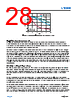
25 / 47 page  Data Sheet LT3046 analog.com Rev 0 25 of 47 The benefit of using a current reference compared to the typical voltage reference used in conventional regulators is that the regulator always operates in a unity-gain configuration, independent of the programmed output voltage. This configuration allows the LT3046 to have loop gain, frequency response, and bandwidth independent of the output voltage. As a result, noise, PSRR, and transient performance do not change with output voltage. Moreover, because none of the error-amplifier gain is needed to amplify the SET pin voltage to a higher output voltage, output load regulation is more tightly specified in the hundreds of microvolts range and not as a fixed percentage of the output voltage. Because the zero temperature-coefficient current source is highly accurate, the SET pin resistor can become a limiting factor in achieving high accuracy. Therefore, the SET pin resistor must be a precision resistor. Additionally, any leakage paths to or from the SET pin create errors in the output voltage. If necessary, use high-quality insulation (for example, Teflon™ or KEL-F®). Moreover, cleaning of all insulating surfaces to remove fluxes and other residues can be required. High humidity environments can require a surface coating at the SET pin to provide a moisture barrier. Minimize board leakage by encircling the SET pin with a guard ring that operates at a potential close to itself, ideally connected to the OUT pins. Guarding both sides of the circuit board is recommended. Bulk leakage reduction depends on the guard-ring width. Leakages of 100nA into or out of the SET pin creates a 0.1% error in the reference voltage. Leakages of this magnitude, coupled with other sources of leakage, can cause significant errors in the output voltage, especially over a wide operating temperature range. Figure 68 illustrates a typical guard-ring layout technique. Figure 68. DFN Guard Ring Layout Because the SET pin is a high-impedance node, unwanted signals can couple into the SET pin and cause erratic behavior, which is most noticeable when operating with a minimum output capacitor at heavy load currents. Bypassing the SET pin with a small capacitance to ground resolves this issue, 10nF is sufficient. For applications requiring higher accuracy or an adjustable output voltage, the SET pin can be actively driven by an external voltage source capable of sinking 100μA. Connecting a precision-voltage reference to the SET pin eliminates any errors present in the output voltage due to the reference current and SET pin resistor tolerances. Output Sensing and Stability The OUTS pin of the LT3046 provides a Kelvin-sense connection to the output. The GND side of the SET pin resistor provides a Kelvin-sense connection to the GND side of the load. Additionally, for ultra-high PSRR, the LT3046 bandwidth is made quite high (~1 MHz), making it close to the self- resonance frequency (~2.3 MHz) of a typical 4.7μF (1206 case size), ceramic, output capacitor. Therefore, it is important to avoid adding extra impedance (ESR and ESL) outside the feedback loop. To that end, as shown in Figure 69, minimize the effects of PCB trace and solder inductance by connecting the OUTS pin directly to COUT and the GND side of CSET directly to the GND side of COUT. Also keep the GND sides of CIN and COUT reasonably close. Refer to the LT3046 evaluation board user guide (LT3046EVK#DFN) for more information on the recommended layout that 1 2 3 4 5 6 7 8 9 10 11 12 13 SET OUT |
|
Ligação URL |
| ALLDATASHEET é útil para você? [ DONATE ] |
Sobre Alldatasheet | Publicidade | Contato conosco | Privacy Policy | Link para a ficha técnica | roca de Link | Lista de Fabricantes All Rights Reserved©Alldatasheet.com |
| Russian : Alldatasheetru.com | Korean : Alldatasheet.co.kr | Spanish : Alldatasheet.es | French : Alldatasheet.fr | Italian : Alldatasheetit.com Portuguese : Alldatasheetpt.com | Polish : Alldatasheet.pl | Vietnamese : Alldatasheet.vn Indian : Alldatasheet.in | Mexican : Alldatasheet.com.mx | British : Alldatasheet.co.uk | New Zealand : Alldatasheet.co.nz |
|
Family Site : ic2ic.com |
icmetro.com |
 Portuguese ▼
 English
 Chinese
 German
 Japanese
 Russian
 Korean
 Spanish
 French
 Italian
 Portuguese
 Polish
 Vietnamese
 Indian
 Mexican
 British
 New Zealand