|
Os motores de busca de Datasheet de Componentes eletrônicos |
|
|
Os motores de busca de Datasheet de Componentes eletrônicos |
|
ADP151 Folha de dados(PDF) 24 Page - Analog Devices |
|
|
|||||||||||||||||||||||||||||
ADP151 Folha de dados(HTML) 24 Page - Analog Devices |
|
|
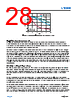
24 / 47 page  Data Sheet LT3046 analog.com Rev 0 24 of 47 APPLICATIONS INFORMATION The LT3046 is a high-performance, low-dropout, linear regulator featuring Analog Devices’ ultra-low noise (2.2nV/√Hz at 10kHz) and ultra-high PSRR (82dB at 1MHz) architecture for powering noise-sensitive applications. Designed as a precision current source followed by a high-performance rail-to-rail voltage buffer, the LT3046 can be easily paralleled to further reduce noise, increase output current, and spread heat on the PCB. The device additionally features programmable current limit, fast start-up capability, and programmable power good. The LT3046 is easy to use and incorporates all of the protection features expected in high-performance regulators. Included are short-circuit protection, safe operating area protection, reverse-battery protection, reverse-current protection, and thermal shutdown with hysteresis. Output Voltage The LT3046 incorporates a precision 100μA current source flowing out of the SET pin, which also connects to the inverting input of the error amplifier. Figure 67 illustrates that connecting a resistor from SET to ground generates a reference voltage for the error amplifier. This reference voltage is the product of the SET pin current and the SET pin resistor. The unity-gain configuration of the error amplifier produces a low-impedance version of this voltage on its noninverting input, that is, the OUTS pin, which is externally connected to the OUT pin. Figure 67. Basic Adjustable Regulator The rail-to-rail error amplifier and current reference of the LT3046 allows for a wide output-voltage range from 0.2V to VIN minus dropout, up to 19V. A PNP-based input pair is active for a 0.2V to ~0.95V output and an NPN-based input pair is active for output voltages greater than ~0.95V, with an abrupt transition between the two input pairs at ~0.95V output with approximately 28mV of hysteresis. While the NPN-based input pair is designed to offer the best overall performance, see Table 1 for details on the offset voltage, SET pin current, output noise, and PSRR variation with the error-amplifier input pair. Table 5 lists many common output voltages and their corresponding 1% RSET resistors. Table 5. 1% Resistor for Common Output Voltages VOUT (V) RSET (kΩ) 2.5 24.9 3.3 33.2 5 49.9 12 121 15 150 18 180 4.7µF 4.7µF 0.47µF 33.2kΩ 100µA IN EN/UV PGFB VIN 5V ±5% SET GND ILIM OUTS OUT LT3046 VOUT 3.3V IOUT(MAX) 200mA PG |
|
Ligação URL |
| ALLDATASHEET é útil para você? [ DONATE ] |
Sobre Alldatasheet | Publicidade | Contato conosco | Privacy Policy | Link para a ficha técnica | roca de Link | Lista de Fabricantes All Rights Reserved©Alldatasheet.com |
| Russian : Alldatasheetru.com | Korean : Alldatasheet.co.kr | Spanish : Alldatasheet.es | French : Alldatasheet.fr | Italian : Alldatasheetit.com Portuguese : Alldatasheetpt.com | Polish : Alldatasheet.pl | Vietnamese : Alldatasheet.vn Indian : Alldatasheet.in | Mexican : Alldatasheet.com.mx | British : Alldatasheet.co.uk | New Zealand : Alldatasheet.co.nz |
|
Family Site : ic2ic.com |
icmetro.com |
 Portuguese ▼
 English
 Chinese
 German
 Japanese
 Russian
 Korean
 Spanish
 French
 Italian
 Portuguese
 Polish
 Vietnamese
 Indian
 Mexican
 British
 New Zealand