|
Os motores de busca de Datasheet de Componentes eletrônicos |
|
|
Os motores de busca de Datasheet de Componentes eletrônicos |
|
ADP151 Folha de dados(PDF) 35 Page - Analog Devices |
|
|
|||||||||||||||||||||||||||||
ADP151 Folha de dados(HTML) 35 Page - Analog Devices |
|
|
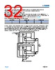
35 / 47 page  Data Sheet LT3046 analog.com Rev 0 35 of 47 Overload Recovery Like many IC power regulators, the LT3046 incorporates SOA protection. The SOA protection activates at input-to- output differential voltages greater than 11V. The SOA protection decreases the current limit because the input-to- output differential increases and keeps the power transistor inside a safe operating region for all values of input-to- output voltages up to the Absolute Maximum Ratings of the LT3046. The LT3046 provides some level of output current for all values of input-to-output differentials. See Figure 32. When power is first applied and the input voltage rises, the output follows the input and keeps the input-to-output differential low to allow the LDO regulator to supply the large output current and startup into high-current loads. Due to current-limit foldback, however, at high-input voltages, a problem can occur if the output voltage is low, and the load current is high. Such situations occur after the removal of a short-circuit or if the EN/UV pin is pulled high after the input voltage is already turned on. The load-line in such cases intersects the output-current profile at two points. The regulator now has two stable operating points. With this double intersection, the input-power supply may need to be cycled down to zero and brought back up again to allow the output to recover. Other LDO regulators with foldback current-limit protection (such as the LT1965 and LT1963A) also exhibit this phenomenon; therefore, it is not unique to the LT3046. Protection Features The LT3046 incorporates several protection features for battery-powered applications. Precision current-limit and thermal-overload protection protect the LT3046 against overload and fault conditions at the output of the device. For normal operation, do not allow the junction temperature to exceed +125°C. To protect the low-noise error amplifier of the LT3046, the SET-to-OUTS protection clamp limits the maximum voltage between SET and OUTS with a maximum DC current of 20mA through the clamp. Therefore, for applications where SET is actively driven by a voltage source, the voltage source must be current limited to 20mA or less. Moreover, to limit the transient current flowing through these clamps during a transient fault condition, limit the maximum value of the SET pin capacitor (CSET) to 22μF. The LT3046 also incorporates reverse-input protection whereby the IN pin withstands reverse voltages of up to -20V without causing any input-current flow and without developing negative voltages at the OUT pin. The regulator protects both itself and the load against batteries that are plugged in backwards. In circuits where a backup battery is required, several different input and output conditions can occur. The output voltage can be held up while the input is either pulled to GND, pulled to some intermediate voltage, or left open- circuit. In all cases, the reverse-current protection circuitry prevents current flow from the output to the input. Nonetheless, due to the OUTS-to-SET clamp, unless the SET pin is floating, current can flow to GND through the SET pin resistor as well as up to 15mA to GND through the output overshoot recovery circuitry. This current flow through the output overshoot recovery circuitry can be significantly reduced by placing a Schottky diode between the OUTS and SET pins, with its anode at the OUTS pin. |
|
Ligação URL |
| ALLDATASHEET é útil para você? [ DONATE ] |
Sobre Alldatasheet | Publicidade | Contato conosco | Privacy Policy | Link para a ficha técnica | roca de Link | Lista de Fabricantes All Rights Reserved©Alldatasheet.com |
| Russian : Alldatasheetru.com | Korean : Alldatasheet.co.kr | Spanish : Alldatasheet.es | French : Alldatasheet.fr | Italian : Alldatasheetit.com Portuguese : Alldatasheetpt.com | Polish : Alldatasheet.pl | Vietnamese : Alldatasheet.vn Indian : Alldatasheet.in | Mexican : Alldatasheet.com.mx | British : Alldatasheet.co.uk | New Zealand : Alldatasheet.co.nz |
|
Family Site : ic2ic.com |
icmetro.com |
 Portuguese ▼
 English
 Chinese
 German
 Japanese
 Russian
 Korean
 Spanish
 French
 Italian
 Portuguese
 Polish
 Vietnamese
 Indian
 Mexican
 British
 New Zealand