|
Os motores de busca de Datasheet de Componentes eletrônicos |
|
|
Os motores de busca de Datasheet de Componentes eletrônicos |
|
ADP151 Folha de dados(PDF) 6 Page - Analog Devices |
|
|
|||||||||||||||||||||||||||||
ADP151 Folha de dados(HTML) 6 Page - Analog Devices |
|
|
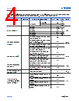
6 / 47 page  Data Sheet LT3046 analog.com Rev 0 6 of 47 (TJ = -40°C to +125°C for the minimum and maximum values, TA = +25°C for the typical values, output capacitance (COUT) = 4.7µF ceramic capacitor, and SET capacitance (CSET) = 4.7µF, unless otherwise noted.) PARAMETER SYMBOL CONDITIONS/COMMENTS MIN TYP MAX UNITS Thermal Shutdown TJ rising +165 °C Hysteresis 6 Start-Up Time VOUT(NOM) = 5V, IL = 200mA, CSET = 0.47µF, VIN = 6V, VPGFB = 6V 55 ms VOUT(NOM) = 5V, IL = 200mA, CSET = 4.7µF, VIN = 6V, VPGFB = 6V 550 VOUT(NOM) = 5V, IL = 200mA, CSET = 4.7µF, VIN = 6V, RPG1 = 50kΩ, RPG2 = 700kΩ (with fast startup to 90% of VOUT) 10 Thermal Regulation 10ms pulse -0.01 %/W . 1 The EN/UV pin threshold must be met to ensure device operation. 2 The maximum TJ limits operating conditions. The regulated output-voltage specification does not apply for all possible combinations of input voltage and output current, especially due to the internal current-limit foldback, which starts to decrease current limit at VIN - VOUT > 11 V. If operating at the maximum output current, limit the input-voltage range. If operating at the maximum input voltage, limit the output-current range. 3 OUTS ties directly to OUT. 4 Changes in ISET and VOS with VSET are tested at 0.2V, 0.75V, 1.3V, and 19V to ensure operation over the 0.2V to 19V SET pin voltage range. 5 The dropout voltage is the minimum input-to-output differential voltage needed to maintain regulation at a specified output current. The dropout voltage is measured when output is 1% out of regulation. This definition results in a higher dropout voltage compared to hard dropout, which is measured when VIN = VOUT(NOMINAL). For output voltages less than 1.7V, the dropout voltage is limited by the minimum input-voltage specification. See Figure 18 for the dropout voltage as a function of the output current and for temperature, see Figure 19, which was measured in a typical application circuit. 6 The GND pin current is tested with VIN = VOUT(NOMINAL) and a current source load. Therefore, the LT3046 is tested while operating in dropout, which is the worst-case GND pin current. The GND pin current decreases at higher input voltages. Note that the GND pin current does not include the SET pin or the ILIM pin current; however, quiescent current does include the SET and ILIM pins. 7 Adding a capacitor across the SET pin resistor decreases the output voltage noise. Adding this capacitor bypasses the thermal noise of the resistor on the SET pin as well as the noise of the reference current. The output noise then equals the error-amplifier noise. Use of a SET pin bypass capacitor also increases the start-up time. 8 The internal back-up current-limit circuitry incorporates foldback protection that decreases current limit for VIN - VOUT > 11 V. Some level of output current is provided at all VIN - VOUT differential voltages. See Figure 32 for the current limit as a function of VIN - VOUT. |
|
Ligação URL |
| ALLDATASHEET é útil para você? [ DONATE ] |
Sobre Alldatasheet | Publicidade | Contato conosco | Privacy Policy | Link para a ficha técnica | roca de Link | Lista de Fabricantes All Rights Reserved©Alldatasheet.com |
| Russian : Alldatasheetru.com | Korean : Alldatasheet.co.kr | Spanish : Alldatasheet.es | French : Alldatasheet.fr | Italian : Alldatasheetit.com Portuguese : Alldatasheetpt.com | Polish : Alldatasheet.pl | Vietnamese : Alldatasheet.vn Indian : Alldatasheet.in | Mexican : Alldatasheet.com.mx | British : Alldatasheet.co.uk | New Zealand : Alldatasheet.co.nz |
|
Family Site : ic2ic.com |
icmetro.com |
 Portuguese ▼
 English
 Chinese
 German
 Japanese
 Russian
 Korean
 Spanish
 French
 Italian
 Portuguese
 Polish
 Vietnamese
 Indian
 Mexican
 British
 New Zealand