|
Os motores de busca de Datasheet de Componentes eletrônicos |
|
|
Os motores de busca de Datasheet de Componentes eletrônicos |
|
LTC3602 Folha de dados(PDF) 20 Page - Linear Technology |
|
|
|||||||||||||||||||||||||||||
LTC3602 Folha de dados(HTML) 20 Page - Linear Technology |
|
|
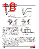
20 / 28 page  LTC3633A-2/LTC3633A-3 20 3633a23f APPLICATIONS INFORMATION As an example, consider the case when one of the regu- lators is used in an application where VIN = SVIN = 12V, IOUT=2A,frequency=2MHz,VOUT=1.8V.FromtheRDS(ON) graphs in the Typical Performance Characteristics section, the top switch on-resistance is nominally 145mΩ and the bottom switch on-resistance is nominally 70mΩ at 70°C ambient. The equivalent power MOSFET resistance RSW is: RDS(ON)TOP • 1.8V 12V +RDS(ON)BOT • 10.2V 12V = 81.3mΩ From the previous section’s discussion on gate drive, we estimate the total gate drive current through the LDO to be 2MHz • 2.3nC = 4.6mA, and IQ of one channel is 0.65mA (see Electrical Characteristics). Therefore, the total power dissipated by a single regulator is: PD = IOUT2 • RSW + SVIN • (IGATECHG + IQ) PD = (2A)2 • (0.0813Ω) + (12V) • (4.6mA + 0.65mA) = 0.388W Running two regulators under the same conditions would result in a power dissipation of 0.776W. The QFN 5mm × 4mm package junction-to-ambient thermal resistance, θJA, is around 43°C/W. Therefore, the junction temperature of the regulator operating in a 70°C ambient temperature is approximately: TJ = 0.776W • 43°C/W + 70°C = 103°C which is below the maximum junction temperature of 125°C. With higher ambient temperatures, a heat sink or cooling fan should be considered to drop the junc- tion-to-ambient thermal resistance. Alternatively, the TSSOP package may be a better choice for high power applications, since it has better thermal properties than the QFN package. Remembering that the above junction temperature is obtained from an RDS(ON) at 70°C, we might recalculate the junction temperature based on a higher RDS(ON) since it increases with temperature. Redoing the calculation assuming that RSW increased 12% at 103°C yields a new junction temperature of 107°C. If the application calls for a higher ambient temperature and/or higher load currents, care should be taken to reduce the temperature rise of the part by using a heat sink or air flow. Figure 8. Temperature Derating Curve for DC1347 Demo Circuit Figure 8 is a temperature derating curve based on the DC1347 demo board (QFN package). It can be used to estimate the maximum allowable ambient temperature for given DC load currents in order to avoid exceeding the maximum operating junction temperature of 125°C. 0 0.5 1.0 1.5 2.0 3.0 2.5 50 125 3633a23 F08 0 3.5 25 75 100 MAXIMUM ALLOWABLE AMBIENT TEMPERATURE (°C) CH2 LOAD = 0A CH2 LOAD = 1A CH2 LOAD = 2A CH2 LOAD = 3A Junction Temperature Measurement The junction-to-ambient thermal resistance will vary de- pending on the size and amount of heat sinking copper on the PCB board where the part is mounted, as well as the amount of air flow on the device. In order to properly evaluate this thermal resistance, the junction temperature needs to be measured. A clever way to measure the junction temperature directly is to use the internal junction diode on one of the pins (PGOOD) to measure its diode voltage change based on ambient temperature change. First remove any external passive component on the PGOOD pin, then pull out 100μA from the PGOOD pin to turn on its internal junction diode and bias the PGOOD pin to a negative voltage. With no output current load, measure the PGOOD voltage at an ambient temperature of 25°C, 75°C and 125°C to establish a slope relationship between the delta voltage on PGOOD and delta ambient temperature. Once this slope is es- tablished,thenthejunction temperaturerisecanbemeasured asafunctionofpowerlossinthepackagewithcorresponding output load current. Although making this measurement with this method does violate absolute maximum voltage ratings on the PGOOD pin, the applied power is so low that there should be no significant risk of damaging the device. |
|
Ligação URL |
| ALLDATASHEET é útil para você? [ DONATE ] |
Sobre Alldatasheet | Publicidade | Contato conosco | Privacy Policy | Link para a ficha técnica | roca de Link | Lista de Fabricantes All Rights Reserved©Alldatasheet.com |
| Russian : Alldatasheetru.com | Korean : Alldatasheet.co.kr | Spanish : Alldatasheet.es | French : Alldatasheet.fr | Italian : Alldatasheetit.com Portuguese : Alldatasheetpt.com | Polish : Alldatasheet.pl | Vietnamese : Alldatasheet.vn Indian : Alldatasheet.in | Mexican : Alldatasheet.com.mx | British : Alldatasheet.co.uk | New Zealand : Alldatasheet.co.nz |
|
Family Site : ic2ic.com |
icmetro.com |
 Portuguese ▼
 English
 Chinese
 German
 Japanese
 Russian
 Korean
 Spanish
 French
 Italian
 Portuguese
 Polish
 Vietnamese
 Indian
 Mexican
 British
 New Zealand