|
Os motores de busca de Datasheet de Componentes eletrônicos |
|
|
Os motores de busca de Datasheet de Componentes eletrônicos |
|
LTC3602 Folha de dados(PDF) 16 Page - Linear Technology |
|
|
|||||||||||||||||||||||||||||
LTC3602 Folha de dados(HTML) 16 Page - Linear Technology |
|
|
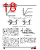
16 / 28 page  LTC3633A-2/LTC3633A-3 16 3633a23f APPLICATIONS INFORMATION Conversely, the minimum on-time is the smallest dura- tion of time in which the top power MOSFET can be in its “on” state. This time is typically 20ns. In continuous mode operation, the minimum on-time limit imposes a minimum duty cycle of: DC(MIN) = f• tON(MIN) () where tON(MIN) is the minimum on-time. As the equation shows, reducing the operating frequency will alleviate the minimum duty cycle constraint. In the rare cases where the minimum duty cycle is surpassed, the output voltage will still remain in regula- tion, but the switching frequency will decrease from its programmed value. This constraint may not be of critical importance in most cases, so high switching frequencies may be used in the design without any fear of severe consequences. As the sections on Inductor and Capacitor selection show, high switching frequencies allow the use of smaller board components, thus reducing the footprint of the application circuit. Internal/External Loop Compensation The LTC3633A-2 provides the option to use a fixed internal loop compensation network to reduce both the required external component count and design time. The internal loop compensation network can be selected by connect- ing the ITH pin to the INTVCC pin. To ensure stability it is recommended that internal compensation only be used with applications with fSW > 1MHz. Alternatively, the user may choose specific external loop compensation components to optimize the main control loop transient response as desired. External loop compensation is chosen by simply connecting the desired network to the ITH pin. Suggested compensation component values are shown in Figure 4. For a 2MHz application, an R-C network of 220pF and 13kΩ provides a good starting point. The bandwidth of the loop increases with decreasing C. If R is increased by the same factor that C is decreased, the zero frequency will be kept the same, thereby keeping the phase the same in the most critical frequency range of the feedback loop. A 10pF bypass capacitor on the ITH pin is recommended for the purposes of filtering out high frequency coupling from stray board capacitance. In addition, a feedforward capacitor CF can be added to improve the high frequency response, as previously shown in Figure 3. Capacitor CF provides phase lead by creating a high frequency zero with R2 which improves the phase margin. Figure 4. Compensation Component ITH RCOMP 13k CCOMP 220pF 3633a23 F04 SGND LTC3633A-2 Checking Transient Response The regulator loop response can be checked by observing the response of the system to a load step. When configured for external compensation, the availability of the ITH pin not only allows optimization of the control loop behavior but also provides a DC-coupled and AC filtered closed loop response test point. The DC step, rise time, and settling behavior at this test point reflect the closed loop response. Assuming a predominantly second order system, phase margin and/or damping factor can be estimated using the percentage of overshoot seen at this pin. The ITH external components shown in Figure 4 circuit will provide an adequate starting point for most applica- tions. The series R-C filter sets the dominant pole-zero loop compensation. The values can be modified slightly (from 0.5 to 2 times their suggested values) to optimize transient response once the final PC layout is done and the particular output capacitor type and value have been determined. The output capacitors need to be selected because their various types and values determine the loop gain and phase. An output current pulse of 20% to 100% of full load current having a rise time of ~1μs will produce output voltage and ITH pin waveforms that will give a sense of the overall loop stability without breaking the feedback loop. Switching regulators take several cycles to respond to a step in load current. When a load step occurs, VOUT im- mediately shifts by an amount equal to ΔILOAD • ESR, where ESR is the effective series resistance of COUT. ΔILOAD also begins to charge or discharge COUT generating a feedback error signal used by the regulator to return VOUT to its |
|
Ligação URL |
| ALLDATASHEET é útil para você? [ DONATE ] |
Sobre Alldatasheet | Publicidade | Contato conosco | Privacy Policy | Link para a ficha técnica | roca de Link | Lista de Fabricantes All Rights Reserved©Alldatasheet.com |
| Russian : Alldatasheetru.com | Korean : Alldatasheet.co.kr | Spanish : Alldatasheet.es | French : Alldatasheet.fr | Italian : Alldatasheetit.com Portuguese : Alldatasheetpt.com | Polish : Alldatasheet.pl | Vietnamese : Alldatasheet.vn Indian : Alldatasheet.in | Mexican : Alldatasheet.com.mx | British : Alldatasheet.co.uk | New Zealand : Alldatasheet.co.nz |
|
Family Site : ic2ic.com |
icmetro.com |
 Portuguese ▼
 English
 Chinese
 German
 Japanese
 Russian
 Korean
 Spanish
 French
 Italian
 Portuguese
 Polish
 Vietnamese
 Indian
 Mexican
 British
 New Zealand