|
Os motores de busca de Datasheet de Componentes eletrônicos |
|
|
Os motores de busca de Datasheet de Componentes eletrônicos |
|
CC1010-RTY1 Folha de dados(PDF) 42 Page - Texas Instruments |
|
|
|||||||||||||||||||||||||||||
CC1010-RTY1 Folha de dados(HTML) 42 Page - Texas Instruments |
|
|
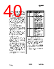
42 / 150 page  CC1010 SWRS047A Page 42 of 146 15.12.12 Programming the Flash Memory After the initialisation is completed, SPI programming can be performed as follows: • Device identity can be verified using the Read Signature Byte instruction. • Perform Chip Erase. • Load one page into the buffer using the Load Program Memory Page instruction. • Write the buffer to Flash by using the Write Program Memory Page instruction. • Repeat the loading and writing of each new page. • Programming can be verified using the Read Program Memory instruction. • Set the lock bits using the Write Lock Bits instruction. • Lock bits can be verified by using the Read Lock Bits instruction. 15.13 8051 Flash Programming Each of the 256 pages (128 bytes each) in Flash program memory can be programmed individually from the 8051. The 8051 must be set in Idle Mode while programming the Flash, since it has no access to the program memory while the writing is in progress. The step for writing a page to Flash is described as follows: • Set the correct write cycle time, according to the current crystal oscillator frequency, in the FLTIM SFR. This number is used to generate the timing to the on-chip Flash interface, as was also done with SPI Flash programming. It must be set so that: MHz f MHz f XOSC XOSC 4 . 0 8 . 0 ≤ ≤ FLTIM • The time used for programming a Flash page is strongly dependent on the setting in FLTIM. It is therefore recommended to set FLTIM as low as possible, as with the SPI Flash programming. • Write the desired Flash page number to the FLADR register. • Disable all interrupts except the Flash / Debug interrupt, which must be enabled (through EICON.FDIE). • Store the 128 bytes of data to be written in the external data memory. The address of the first byte in the buffer must be a multiple of 128. • Write the 4 most significant bits of the RAM buffer address to FLCON.RMADR(3:0) . Also set the bit FLCON.WRFLASH. • Set the 8051 in Idle Mode by setting PCON.IDLE . The Flash page is then automatically erased and programmed. The sequence of the above steps is not important. Flash programming is started whenever entering Idle Mode while FLCON.WRFLASH is set. A Flash / Debug interrupt will be generated when the page write operation is completed, which will get the 8051 out of Idle Mode. An ISR must be present to service the Flash / Debug interrupt. |
|
Ligação URL |
| ALLDATASHEET é útil para você? [ DONATE ] |
Sobre Alldatasheet | Publicidade | Contato conosco | Privacy Policy | Link para a ficha técnica | roca de Link | Lista de Fabricantes All Rights Reserved©Alldatasheet.com |
| Russian : Alldatasheetru.com | Korean : Alldatasheet.co.kr | Spanish : Alldatasheet.es | French : Alldatasheet.fr | Italian : Alldatasheetit.com Portuguese : Alldatasheetpt.com | Polish : Alldatasheet.pl | Vietnamese : Alldatasheet.vn Indian : Alldatasheet.in | Mexican : Alldatasheet.com.mx | British : Alldatasheet.co.uk | New Zealand : Alldatasheet.co.nz |
|
Family Site : ic2ic.com |
icmetro.com |
 Portuguese ▼
 English
 Chinese
 German
 Japanese
 Russian
 Korean
 Spanish
 French
 Italian
 Portuguese
 Polish
 Vietnamese
 Indian
 Mexican
 British
 New Zealand