|
Os motores de busca de Datasheet de Componentes eletrônicos |
|
|
Os motores de busca de Datasheet de Componentes eletrônicos |
|
CC1010-RTY1 Folha de dados(PDF) 15 Page - Texas Instruments |
|
|
|||||||||||||||||||||||||||||
CC1010-RTY1 Folha de dados(HTML) 15 Page - Texas Instruments |
|
|
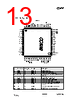
15 / 150 page  CC1010 SWRS047A Page 15 of 146 Pin # Pin name Alternate function Pin type Description 51 P0.2 MI (I) SO (O) Digital high-Z I/O 8051 port 0, bit 2 or SPI interface master input or Flash programming SPI slave serial data output 52 P0.3 - Digital high-Z I/O 8051 port 0, bit 3 53 P1.5 - Digital high-Z I/O 8051 port 1, bit 5 54 P1.6 - Digital high-Z I/O 8051 port 1, bit 6 55 P1.7 - Digital high-Z I/O 8051 port 1, bit 7 56 P2.6 - Digital high-Z I/O 8051 port 2, bit 6 57 P2.7 - Digital high-Z I/O 8051 port 2, bit 7 58 PROG - Digital input Flash program enable pad, active low 59 RESET - Digital input (pull-up) System reset pin, active low 60 DVDD - Power (D) Digital power supply 61 AD0 - Analog input ADC input channel 0 62 AD1 - Analog input ADC input channel 1 63 AD2 RSSI (O), IF (O) Analog input/output ADC input channel 2, RSSI (Receiver signal strength indicator) output, or IF output when using external demodulator 64 AGND - Power (A) Analog ground connection ADC A = Analog, D = Digital, I = input, O= Output 13. Pin description AVDD, DVDD Supply voltages for analog and digital modules respectively. All supply pins should be decoupled by capacitors. In particular, the digital and analog supply domains should be properly decoupled from each other (a ferrite bead can be used to prevent high-frequency noise from coupling from one supply domain to another). The placement and size of decoupling capacitors and supply filtering are critical with respect to LO leakage and sensitivity. Chipcon’s reference layout designs should be used (available from Chipcon’s website). See also page 133 for layout recommendations. AGND, DGND Ground for analog and digital modules respectively. Normally one common ground plane is recommended. If two separate analog and digital grounds are used they should be interconnected in one place, and one place only. RFIN This is the RF input, internally connected to the low noise amplifier (LNA). The signal source (antenna) should be matched to the input impedance. A DC ground is needed for LNA biasing. RFOUT This is the RF output, internally connected to the power amplifier (PA). The external load (antenna) should be matched to the output impedance (optimum load impedance). This pin must be DC coupled to AVDD for PA biasing (open drain output). L1, L2 Connection to internal voltage controlled oscillator (VCO). An inductor should be connected between these pins. The inductor value will determine the VCO tuning range. The inductor should be place very close to the pins in order to minimize paracitic inductance. CHP_OUT Charge Pump output. If the RF transceiver is configured for external loop filter this is the current output from the charge pump. Normally the internal loop filter should be used and this pin should be left open (not connected). |
|
Ligação URL |
| ALLDATASHEET é útil para você? [ DONATE ] |
Sobre Alldatasheet | Publicidade | Contato conosco | Privacy Policy | Link para a ficha técnica | roca de Link | Lista de Fabricantes All Rights Reserved©Alldatasheet.com |
| Russian : Alldatasheetru.com | Korean : Alldatasheet.co.kr | Spanish : Alldatasheet.es | French : Alldatasheet.fr | Italian : Alldatasheetit.com Portuguese : Alldatasheetpt.com | Polish : Alldatasheet.pl | Vietnamese : Alldatasheet.vn Indian : Alldatasheet.in | Mexican : Alldatasheet.com.mx | British : Alldatasheet.co.uk | New Zealand : Alldatasheet.co.nz |
|
Family Site : ic2ic.com |
icmetro.com |
 Portuguese ▼
 English
 Chinese
 German
 Japanese
 Russian
 Korean
 Spanish
 French
 Italian
 Portuguese
 Polish
 Vietnamese
 Indian
 Mexican
 British
 New Zealand