|
Os motores de busca de Datasheet de Componentes eletrônicos |
|
|
Os motores de busca de Datasheet de Componentes eletrônicos |
|
LTC1291 Folha de dados(PDF) 15 Page - Linear Technology |
|
|
|||||||||||||||||||||||||||||
LTC1291 Folha de dados(HTML) 15 Page - Linear Technology |
|
|
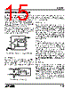
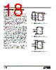
15 / 20 page  15 LTC1291 S APPLICATI I FOR ATIO or GND lead will cause gain errors and offset errors (Figure 7). For the best performance the LTC1291 should be soldered directly to the PC board. If the source can not be placed next to the pin and the gain parameter is important the pin should be Kelvin-sensed to eliminate parasitic resistances due to long PC traces. For example, 0.1 Ω of resistance in the VCC lead can typically cause 0.5LSB (ICC × 0.1Ω/VCC) of gain error for VCC = 5V. When the input MUX is selected for single-ended input the minus terminal is connected to GND internally on the die. Any parasitic resistance from the GND pin to the ground plane will lead to an offset voltage (ICC × RP2). “+” Input Settling The input capacitor is switched onto the “+” input during the sample phase (tSMPL, see Figure 9). The sample period is 2.5 CLK cycles before a conversion starts. The voltage on the “+” input must settle completely within the sample period. Minimizing RSOURCE+ and C1 will improve the settling time. If large “+” input source resistance must be used, the sample time can be increased by using a slower CLK frequency. With the minimum possible sample time of 2.5 µs, RSOURCE+ < 1.0k and C1 < 20pF will provide adequate settle time. “–” Input Settling At the end of the sample phase the input capacitor switches to the “–” input and the conversion starts (see Figure 9). During the conversion, the “+” input voltage is effectively “held” by the sample-and-hold and will not affect the conversion result. It is critical that the “–” input voltage be free of noise and settle completely during the first CLK cycle of the conversion. Minimizing RSOURCE– and C2 will improve settling time. If large “–” input source resistance must be used, the time can be extended by using a slower CLK frequency. At the maximum CLK frequency of 1MHz, RSOURCE– < 250Ω and C2 < 20pF will provide adequate settling. Input Op Amps When driving the analog inputs with an op amp it is important that the op amp settles within the allowed time (see Figure 9). Again the “+” and “–” input sampling times can be extended as described above to accommodate slower op amps. Most op amps including the LT1006 and LT1013 single supply op amps can be made to settle well even with the minimum settling windows of 2.5 µs (“+” input) and 1 µs (“–” input) that occurs at the maximum clock rate of 1MHz. Figures 10 and 11 show examples adequate and poor op amp settling. and capacitances will slow the settling of the inputs. It is important that the overall RC time constant is short enough to allow the analog inputs to settle completely within the allowed time. Figure 7. Parasitic Resistance in the VCC and GND Leads Source Resistance The analog inputs of the LTC1291 look like a 100pF capacitor (CIN) in series with a 500Ω resistor (RON). CIN gets switched between “+” and “–” inputs once during each conversion cycle. Large external source resistors Figure 8. Analog Input Equivalent Circuit REF+ REF– D/A 5V VCC GND LTC1291 F07 RP1 RP2 LTC1291 3RD CLK ↑ RON = 500Ω CIN = 100pF LTC1291 “+” INPUT RSOURCE + VIN + C1 “–” INPUT RSOURCE – VIN – C2 LTC1291 F08 5TH CLK ↓ |
|
|
Ligação URL |
| ALLDATASHEET é útil para você? [ DONATE ] |
Sobre Alldatasheet | Publicidade | Contato conosco | Privacy Policy | Link para a ficha técnica | roca de Link | Lista de Fabricantes All Rights Reserved©Alldatasheet.com |
| Russian : Alldatasheetru.com | Korean : Alldatasheet.co.kr | Spanish : Alldatasheet.es | French : Alldatasheet.fr | Italian : Alldatasheetit.com Portuguese : Alldatasheetpt.com | Polish : Alldatasheet.pl | Vietnamese : Alldatasheet.vn Indian : Alldatasheet.in | Mexican : Alldatasheet.com.mx | British : Alldatasheet.co.uk | New Zealand : Alldatasheet.co.nz |
|
Family Site : ic2ic.com |
icmetro.com |
 Portuguese ▼
 English
 Chinese
 German
 Japanese
 Russian
 Korean
 Spanish
 French
 Italian
 Portuguese
 Polish
 Vietnamese
 Indian
 Mexican
 British
 New Zealand