|
Os motores de busca de Datasheet de Componentes eletrônicos |
|
|
Os motores de busca de Datasheet de Componentes eletrônicos |
|
SSM2537ACBZ-R7 Folha de dados(PDF) 14 Page - Analog Devices |
|
|
|||||||||||||||||||||||||||||
SSM2537ACBZ-R7 Folha de dados(HTML) 14 Page - Analog Devices |
|
|
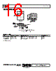
14 / 16 page  SSM2537 Data Sheet Rev. 0 | Page 14 of 16 PDM PATTERN CONTROL The SSM2537 has a simple control mechanism that can set the part for low power states and control functionality. This is accomplished by sending a repeating 8-bit pattern to the device. Different patterns set different functionality (see Table 8). Any pattern must be repeated a minimum of 129 times. The part is automatically muted when a pattern is detected so that a pattern can be set while the part is operational without a pop/click due to pattern transition. All functionality set via patterns returns to its default values after a clock-loss power-down. Table 8. PDM Watermarking Pattern Control Descriptions Pattern Control Description 0xD2 Gain optimized for PVDD = 3.6 V operation. 0xD4 Gain optimized for PVDD = 2.5 V operation. 0xD8 Gain optimized for PVDD = 5 V operation. 0xE1 Ultralow EMI mode. 0xE2 Low latency mode with pattern delay (~15 μs latency). 0xE4 fS set to opposite value determined by GAIN_FS pin. 0xAA Device reset: Place device into default configuration. 0x66 Mute. 0xAC Power-down: All blocks off except for PDM interface. Normal start-up time. EMI NOISE The SSM2537 uses a proprietary modulation and spread- spectrum technology to minimize EMI emissions from the device. For applications that have difficulty passing FCC Class B emission tests, the SSM2537 includes a modulation select mode (ultralow EMI emissions mode) that significantly reduces the radiated emissions at the Class-D outputs, particu- larly above 100 MHz. This mode is enabled by activating PDM Watermarking Pattern 0xE1 (see Table 8). PDM CHANNEL SELECTION The SSM2537 includes a left/right input select pin, LRSEL (see Table 9), that determines which of the time-multiplexed input streams is routed to the amplifier. To select the left input channel, connect LRSEL to PGND. To select the right channel, connect LRSEL to VDD. At any point during amplifier operation, the logic level applied to LRSEL may be changed and the output will switch the input streams without audible artifacts. No muting, watermarking pattern or synchronizing are necessary to achieve a click/pop free LRSEL transition. Table 9. LRSEL Pin Function Descriptions Device Setting LRSEL Pin Configuration Right Channel Select VDD Left Channel Select PGND OUTPUT MODULATION DESCRIPTION The SSM2537 uses three-level, Σ-Δ output modulation. Each output can swing from PGND to PVDD and vice versa. Ideally, when no input signal is present, the output differential voltage is 0 V because there is no need to generate a pulse. In a real-world situation, there are always noise sources present. Due to this constant presence of noise, a differential pulse is generated, when required, in response to this stimulus. A small amount of current flows into the inductive load when the differential pulse is generated. Most of the time, however, the output differential voltage is 0 V, due to the Analog Devices, Inc., three-level, Σ-Δ output modulation. This feature ensures that the current flowing through the inductive load is small. When the user wants to send an input signal, an output pulse (OUT+ and OUT−) is generated to follow the input voltage. The differential pulse density (VOUT) is increased by raising the input signal level. Figure 33 depicts three-level, Σ-Δ output modulation with and without input stimulus. Figure 33. Three-Level, Σ-Δ Output Modulation With and Without Input Stimulus OUTPUT > 0V +5V 0V OUT+ +5V 0V OUT– +5V 0V VOUT OUTPUT < 0V +5V 0V OUT+ +5V 0V OUT– 0V –5V VOUT OUTPUT = 0V OUT+ +5V 0V +5V 0V OUT– +5V –5V 0V VOUT |
|
|
Ligação URL |
| ALLDATASHEET é útil para você? [ DONATE ] |
Sobre Alldatasheet | Publicidade | Contato conosco | Privacy Policy | Link para a ficha técnica | roca de Link | Lista de Fabricantes All Rights Reserved©Alldatasheet.com |
| Russian : Alldatasheetru.com | Korean : Alldatasheet.co.kr | Spanish : Alldatasheet.es | French : Alldatasheet.fr | Italian : Alldatasheetit.com Portuguese : Alldatasheetpt.com | Polish : Alldatasheet.pl | Vietnamese : Alldatasheet.vn Indian : Alldatasheet.in | Mexican : Alldatasheet.com.mx | British : Alldatasheet.co.uk | New Zealand : Alldatasheet.co.nz |
|
Family Site : ic2ic.com |
icmetro.com |
 Portuguese ▼
 English
 Chinese
 German
 Japanese
 Russian
 Korean
 Spanish
 French
 Italian
 Portuguese
 Polish
 Vietnamese
 Indian
 Mexican
 British
 New Zealand