|
Os motores de busca de Datasheet de Componentes eletrônicos |
|
|
Os motores de busca de Datasheet de Componentes eletrônicos |
|
AT89LS53 Folha de dados(PDF) 18 Page - ATMEL Corporation |
|
|
|||||||||||||||||||||||||||||
AT89LS53 Folha de dados(HTML) 18 Page - ATMEL Corporation |
|
|
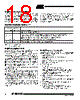
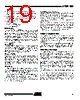
18 / 35 page  AT89LS53 0851C–MICRO–3/06 18 Program Memory Lock Bits The AT89LS53 has three lock bits that can be left unpro- grammed (U) or can be programmed (P) to obtain the addi- tional features listed in the following table. When lock bit 1 is programmed, the logic level at the EA pin is sampled and latched during reset. If the device is pow- ered up without a reset, the latch initializes to a random value and holds that value until reset is activated. The latched value of EA must agree with the current logic level at that pin in order for the device to function properly. Once programmed, the lock bits can only be unpro- grammed with the Chip Erase operations in either the par- allel or serial modes. Lock Bit Protection Modes (1) (2) Notes: 1. U = Unprogrammed 2. P = Programmed Program Lock Bits Protection Type LB1 LB2 LB3 1 U U U No internal memory lock feature. 2 P U U MOVC instructions executed from external program memory are disabled from fetching code bytes from internal memory. EA is sampled and latched on reset and further programming of the Flash memory (parallel or serial mode) is disabled. 3 P P U Same as Mode 2, but parallel or serial verify are also disabled. 4 P P P Same as Mode 3, but external execution is also disabled. Programming the Flash Atmel’s AT89LS53 Flash Microcontroller offers 12K bytes of in-system reprogrammable Flash Code memory. The AT89LS53 is normally shipped with the on-chip Flash Code memory array in the erased state (i.e. contents = FFH) and ready to be programmed. This device supports a High-Voltage (12V) Parallel programming mode and a Low- Voltage (2.7 to 6.0V) Serial programming mode. The serial programming mode provides a convenient way to down- load the AT89LS53 inside the user’s system. The parallel programming mode is compatible with conventional third party Flash or EPROM programmers. The Code memory array occupies one contiguous address space from 0000H to 2FFFH. The Code array on the AT89LS53 is programmed byte-by- byte in either programming mode. An auto-erase cycle is provided with the self-timed programming operation in the serial programming mode. There is no need to perform the Chip Erase operation to reprogram any memory location in the serial programming mode unless any of the lock bits have been programmed. In the parallel programming mode, there is no auto-erase cycle. To reprogram any non-blank byte, the user needs to use the Chip Erase operation first to erase the entire Code memory array. Parallel Programming Algorithm To program and verify the AT89LS53 in the parallel pro- gramming mode, the following sequence is recommended: 1. Power-up sequence: Apply power between VCC and GND pins. Set RST pin to “H”. Apply a 3 MHz to 12 MHz clock to XTAL1 pin and wait for at least 10 milliseconds. 2. Set PSEN pin to “L” ALE pin to “H” EA pin to “H” and all other pins to “H”. 3. Apply the appropriate combination of “H” or “L” logic levels to pins P2.6, P2.7, P3.6, P3.7 to select one of the programming operations shown in the Flash Programming Modes table. 4. Apply the desired byte address to pins P1.0 to P1.7 and P2.0 to P2.5. Apply data to pins P0.0 to P0.7 for Write Code opera- tion. 5. Raise EA/VPP to 12V to enable Flash programming, erase or verification. 6. Pulse ALE/PROG once to program a byte in the Code memory array, or the lock bits. The byte-write cycle is self-timed and typically takes 1.5 ms. |
|
Ligação URL |
| ALLDATASHEET é útil para você? [ DONATE ] |
Sobre Alldatasheet | Publicidade | Contato conosco | Privacy Policy | Link para a ficha técnica | roca de Link | Lista de Fabricantes All Rights Reserved©Alldatasheet.com |
| Russian : Alldatasheetru.com | Korean : Alldatasheet.co.kr | Spanish : Alldatasheet.es | French : Alldatasheet.fr | Italian : Alldatasheetit.com Portuguese : Alldatasheetpt.com | Polish : Alldatasheet.pl | Vietnamese : Alldatasheet.vn Indian : Alldatasheet.in | Mexican : Alldatasheet.com.mx | British : Alldatasheet.co.uk | New Zealand : Alldatasheet.co.nz |
|
Family Site : ic2ic.com |
icmetro.com |
 Portuguese ▼
 English
 Chinese
 German
 Japanese
 Russian
 Korean
 Spanish
 French
 Italian
 Portuguese
 Polish
 Vietnamese
 Indian
 Mexican
 British
 New Zealand