|
Os motores de busca de Datasheet de Componentes eletrônicos |
|
|
Os motores de busca de Datasheet de Componentes eletrônicos |
|
USB2640 Folha de dados(PDF) 16 Page - Microchip Technology |
|
|
|||||||||||||||||||||||||||||
USB2640 Folha de dados(HTML) 16 Page - Microchip Technology |
|
|
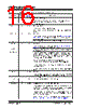
16 / 60 page  USB2640/USB2641 DS00001947C-page 16 2015-2021 Microchip Technology Inc. XTAL2 44 OCLKx 24 MHz Crystal Output This is the other terminal of the crystal, or it is left open when an external clock source is used to drive XTAL1(CLKIN). SPI INTERFACE SPI_CE_n 8 O12 SPI Chip Enable This is the active low chip enable output. When the SPI interface is enabled, drive this pin high in power down states. SPI_CLK / SCL 9 I/O12 SPI Clock This is the SPI clock out to the serial ROM. See Section 6.4, "ROM BOOT Sequence" for diagram and usage instructions. During reset, drive this pin low. When configured, this is the I2C EEPROM clock pin. SPI_DO / SDA / SPI_SPD_SEL 10 I/O12 SPI Data Out This is the data out for the SPI port. See Section 6.4, "ROM BOOT Sequence" for diagram and usage instructions. This pin is the data pin when the device is connected to the optional I2C EEPROM. This pin is used to select the speed of the SPI interface. During nRESET assertion, this pin will be tri-stated with the weak pull-down resistor enabled. When nRESET is negated, the value on the pin will be internally latched, and the pin will revert to SPI_DO functionality, the internal pull-down will be disabled. ‘0’ = 30 MHz (No external resistor should be applied) ‘1’ = 60 MHz (A 10 K external pull-up resistor must be applied) If the latched value is '1', then the pin is tri-stated when the chip is in the suspend state. If the latched value is '0', then the pin is driven low during a suspend state. SPI_DI 11 I/O12PD SPI Data In This is the data in to the controller from the ROM. This pin has a weak internal pull-down applied at all times to prevent floating. MISC LED NC 37 36 I/O12 It can be used as media activities LED output. CRD_PWR 35 I/O200 Card power drive: 3.3 V (100 mA or 200 mA) This pin powers the multiplexed flash media interface (slot) for xD, MS, and SD/MMC. If card power is not being used to power the multiplexed flash media interface, this pin may be used as a GPIO. It is a requirement for this to be the only FET used to power xD-Picture Card devices. Failure to do this will violate xD voltage specification on xD-Picture Card device pins. Bits 0, 1, 2, and 3 control FET 2 of Register A5h. Please reference Section 7.3.4.5, "A8h: LED Blink Interval (1 byte)," on page 30. TABLE 6-1: USB2640/USB2641 PIN DESCRIPTIONS (CONTINUED) Symbol 48-Pin QFN Buffer Type (Table 6-2) Description |
|
Ligação URL |
| ALLDATASHEET é útil para você? [ DONATE ] |
Sobre Alldatasheet | Publicidade | Contato conosco | Privacy Policy | Link para a ficha técnica | roca de Link | Lista de Fabricantes All Rights Reserved©Alldatasheet.com |
| Russian : Alldatasheetru.com | Korean : Alldatasheet.co.kr | Spanish : Alldatasheet.es | French : Alldatasheet.fr | Italian : Alldatasheetit.com Portuguese : Alldatasheetpt.com | Polish : Alldatasheet.pl | Vietnamese : Alldatasheet.vn Indian : Alldatasheet.in | Mexican : Alldatasheet.com.mx | British : Alldatasheet.co.uk | New Zealand : Alldatasheet.co.nz |
|
Family Site : ic2ic.com |
icmetro.com |
 Portuguese ▼
 English
 Chinese
 German
 Japanese
 Russian
 Korean
 Spanish
 French
 Italian
 Portuguese
 Polish
 Vietnamese
 Indian
 Mexican
 British
 New Zealand