Os motores de busca de Datasheet de Componentes eletrônicos
  Portuguese  ▼
ALLDATASHEETPT.COM

X  

LTC1291 Datasheet with Chat AI
  • AIauthorized

    Hello, Please ask a question about LTC1291 Datasheet

  • # Example questions: ➢ What parameters are being measured using the load circuit for 't_dis' and 't_en'?
    ➢ What does sar stand for in this context, and what is its role in the a/d conversion process?
    ➢ What is the primary function of the 'cs' pin on the ltc1291, and what happens when it is asserted (logic low)?

  • Part No.LTC1291
    ManufacturerLINER
    Size376 Kbytes
    Pages20 pages
    DescriptionSingle Chip 12-Bit Data Acquisition System
    Datasheet Summary with AI

    1. Overview

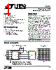
    ️· What it is: The LTC1291 is a 12-bit, 8-channel Analog-to-Digital Converter (ADC) with a sample-and-hold (S/H) function and a serial interface. It's designed for data acquisition in a variety of applications.
    ️· Key Features:
    - 12-bit Resolution: Provides good accuracy in converting analog signals to digital.
    - 8 Channels: Can sample 8 separate analog inputs.
    - Serial Interface: Communicates with a microcontroller or other digital system serially (shifting data in and out).
    - Sample-and-Hold: Captures a snapshot of the analog signal for accurate conversion.
    - Multiplexer: Allows selection of one of the 8 analog input channels.
    - Low Power: Designed for power-sensitive applications.

    2. Pin Descriptions (Key Pins)

    Pin Name Description
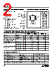
    1/2 CS Chip Select – Enables the ADC. Logic low active.
    3-4 CH0-CH1 Analog Input Channels – Connect to analog signals to be converted.
    5 GND Analog Ground – Must be connected to a good analog ground plane.
    6 DIN Data In – Serial data input.
    7 DOUT Data Out – Serial data output.
    8 CLK Shift Clock – Synchronizes serial data transfer.
    | VCC/VREF | Supply/Reference Voltage – Provides power and defines the conversion range. Needs good bypassing.

    3. Functional Block Diagram

    ️· Key Modules:
    - Analog Input Multiplexer: Selects one of the 8 analog channels.
    - Sample-and-Hold (S/H): Samples the analog voltage.
    - 12-bit SAR (Successive Approximation Register) ADC: Converts the sampled voltage to a 12-bit digital value.
    - 12-bit DAC (Digital-to-Analog Converter): This is used internally for the SAR algorithm.
    - Shift Registers: Handle serial data transfer.
    - Control and Timing Logic: Manages the overall operation.

    4. Operating Characteristics (Important Specs - Not all included but critical for design)

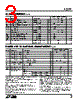
    ️· Resolution: 12 bits
    ️· Number of Channels: 8
    ️· Conversion Time: (Not explicitly stated, but this is a key performance factor that needs to be checked in the full datasheet)
    ️· Input Voltage Range: Determined by VCC and VREF. This needs to be carefully planned.
    ️· Power Supply Voltage (VCC): (Not explicitly stated, check full datasheet)
    ️· On and Off Channel Leakage Current: (Low, but important for high-impedance sensors)

    5. Test Circuits & Waveforms

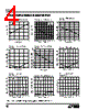
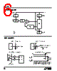
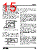
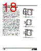
    ️· Load Circuit for t_dDO, t_r and t_f: Shows how to load the data output for timing measurements.
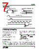
    ️· Voltage Waveforms for t_dis and t_en: Illustrates the data output control signals.
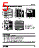
    ️· On and Off Channel Leakage Current: Provides a test circuit for measuring leakage.

    6. Design Considerations & Key Takeaways

    ️· Analog Ground Plane: Absolutely critical for clean operation.
    ️· Bypass Capacitors: Place bypass capacitors close to the VCC/VREF pin to minimize noise and ripple.
    ️· Serial Communication: The serial interface requires careful timing and control signals.
    ️· Input Voltage Range: Make sure the analog input voltages stay within the specified range.
    ️· External Components: May be required for external filtering or buffering, depending on the application.
    ️· Timing: Conversion time and serial communication speed are important design parameters.


    To effectively use this summary:

    ️· Refer to the full datasheet: This summary highlights key points, but the complete datasheet contains detailed specifications, timing diagrams, and application notes that are essential for a successful design.
    ️· Consider the specific application: The design choices will depend on the specific requirements of the application, such as accuracy, speed, and power consumption.
    ️· Check the electrical characteristics: Carefully review the electrical characteristics section to ensure that the LTC1291 meets the application's requirements.

    1. Overview

    ️· What it is: The LTC1291 is a 12-bit, 8-channel Analog-to-Digital Converter (ADC) with a sample-and-hold (S/H) function and a serial interface. It's designed for data acquisition in a variety of applications.
    ️· Key Features:
    - 12-bit Resolution: Provides good accuracy in converting analog signals to digital.
    - 8 Channels: Can sample 8 separate analog inputs.
    - Serial Interface: Communicates with a microcontroller or other digital system serially (shifting data in and out).
    - Sample-and-Hold: Captures a snapshot of the analog signal for accurate conversion.
    - Multiplexer: Allows selection of one of the 8 analog input channels.
    - Low Power: Designed for power-sensitive applications.

    2. Pin Descriptions (Key Pins)

    Pin Name Description
    1/2 CS Chip Select – Enables the ADC. Logic low active.
    3-4 CH0-CH1 Analog Input Channels – Connect to analog signals to be converted.
    5 GND Analog Ground – Must be connected to a good analog ground plane.
    6 DIN Data In – Serial data input.
    7 DOUT Data Out – Serial data output.
    8 CLK Shift Clock – Synchronizes serial data transfer.
    | VCC/VREF | Supply/Reference Voltage – Provides power and defines the conversion range. Needs good bypassing.

    3. Functional Block Diagram

    ️· Key Modules:
    - Analog Input Multiplexer: Selects one of the 8 analog channels.
    - Sample-and-Hold (S/H): Samples the analog voltage.
    - 12-bit SAR (Successive Approximation Register) ADC: Converts the sampled voltage to a 12-bit digital value.
    - 12-bit DAC (Digital-to-Analog Converter): This is used internally for the SAR algorithm.
    - Shift Registers: Handle serial data transfer.
    - Control and Timing Logic: Manages the overall operation.

    4. Operating Characteristics (Important Specs - Not all included but critical for design)

    ️· Resolution: 12 bits
    ️· Number of Channels: 8
    ️· Conversion Time: (Not explicitly stated, but this is a key performance factor that needs to be checked in the full datasheet)
    ️· Input Voltage Range: Determined by VCC and VREF. This needs to be carefully planned.
    ️· Power Supply Voltage (VCC): (Not explicitly stated, check full datasheet)
    ️· On and Off Channel Leakage Current: (Low, but important for high-impedance sensors)

    5. Test Circuits & Waveforms

    ️· Load Circuit for t_dDO, t_r and t_f: Shows how to load the data output for timing measurements.
    ️· Voltage Waveforms for t_dis and t_en: Illustrates the data output control signals.
    ️· On and Off Channel Leakage Current: Provides a test circuit for measuring leakage.

    6. Design Considerations & Key Takeaways

    ️· Analog Ground Plane: Absolutely critical for clean operation.
    ️· Bypass Capacitors: Place bypass capacitors close to the VCC/VREF pin to minimize noise and ripple.
    ️· Serial Communication: The serial interface requires careful timing and control signals.
    ️· Input Voltage Range: Make sure the analog input voltages stay within the specified range.
    ️· External Components: May be required for external filtering or buffering, depending on the application.
    ️· Timing: Conversion time and serial communication speed are important design parameters.


    To effectively use this summary:

    ️· Refer to the full datasheet: This summary highlights key points, but the complete datasheet contains detailed specifications, timing diagrams, and application notes that are essential for a successful design.
    ️· Consider the specific application: The design choices will depend on the specific requirements of the application, such as accuracy, speed, and power consumption.
    ️· Check the electrical characteristics: Carefully review the electrical characteristics section to ensure that the LTC1291 meets the application's requirements.

    Part No.LTC1291
    ManufacturerLINER
    Size376 Kbytes
    Pages20 pages
    DescriptionSingle Chip 12-Bit Data Acquisition System
    ALLDATASHEET é útil para você?  [ DONATE ] 

    Sobre Alldatasheet   |   Publicidade   |   Contato conosco   |   Privacy Policy   |   Link para a ficha técnica    |   roca de Link   |   Lista de Fabricantes
    All Rights Reserved©Alldatasheet.com


    Mirror Sites
    English : Alldatasheet.com  |   English : Alldatasheet.net  |   Chinese : Alldatasheetcn.com  |   German : Alldatasheetde.com  |   Japanese : Alldatasheet.jp
    Russian : Alldatasheetru.com  |   Korean : Alldatasheet.co.kr  |   Spanish : Alldatasheet.es  |   French : Alldatasheet.fr  |   Italian : Alldatasheetit.com
    Portuguese : Alldatasheetpt.com  |   Polish : Alldatasheet.pl  |   Vietnamese : Alldatasheet.vn
    Indian : Alldatasheet.in  |   Mexican : Alldatasheet.com.mx  |   British : Alldatasheet.co.uk  |   New Zealand : Alldatasheet.co.nz
    Family Site : ic2ic.com  |   icmetro.com