|
Os motores de busca de Datasheet de Componentes eletrônicos |
|
|
Os motores de busca de Datasheet de Componentes eletrônicos |
|
PIC18F8720 Folha de dados(PDF) 15 Page - Microchip Technology |
|
|
|||||||||||||||||||||||||||||
PIC18F8720 Folha de dados(HTML) 15 Page - Microchip Technology |
|
|
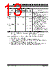
15 / 380 page  2004 Microchip Technology Inc. DS39609B-page 13 PIC18F6520/8520/6620/8620/6720/8720 PORTB is a bidirectional I/O port. PORTB can be software programmed for internal weak pull-ups on all inputs. RB0/INT0 RB0 INT0 48 58 I/O I TTL ST Digital I/O. External interrupt 0. RB1/INT1 RB1 INT1 47 57 I/O I TTL ST Digital I/O. External interrupt 1. RB2/INT2 RB2 INT2 46 56 I/O I TTL ST Digital I/O. External interrupt 2. RB3/INT3/CCP2 RB3 INT3 CCP2(1) 45 55 I/O I/O I/O TTL ST ST Digital I/O. External interrupt 3. Capture2 input, Compare2 output, PWM2 output. RB4/KBI0 RB4 KBI0 44 54 I/O I TTL ST Digital I/O. Interrupt-on-change pin. RB5/KBI1/PGM RB5 KBI1 PGM 43 53 I/O I I/O TTL ST ST Digital I/O. Interrupt-on-change pin. Low-Voltage ICSP Programming enable pin. RB6/KBI2/PGC RB6 KBI2 PGC 42 52 I/O I I/O TTL ST ST Digital I/O. Interrupt-on-change pin. In-Circuit Debugger and ICSP programming clock. RB7/KBI3/PGD RB7 KBI3 PGD 37 47 I/O I/O TTL ST Digital I/O. Interrupt-on-change pin. In-Circuit Debugger and ICSP programming data. TABLE 1-2: PIC18FXX20 PINOUT I/O DESCRIPTIONS (CONTINUED) Pin Name Pin Number Pin Type Buffer Type Description PIC18F6X20 PIC18F8X20 Legend: TTL = TTL compatible input CMOS = CMOS compatible input or output ST = Schmitt Trigger input with CMOS levels Analog = Analog input I = Input O = Output P = Power OD = Open-Drain (no P diode to VDD) Note 1: Alternate assignment for CCP2 when CCP2MX is not selected (all operating modes except Microcontroller). 2: Default assignment when CCP2MX is set. 3: External memory interface functions are only available on PIC18F8X20 devices. 4: CCP2 is multiplexed with this pin by default when configured in Microcontroller mode. Otherwise, it is multiplexed with either RB3 or RC1. 5: PORTH and PORTJ are only available on PIC18F8X20 (80-pin) devices. 6: AVDD must be connected to a positive supply and AVSS must be connected to a ground reference for proper operation of the part in user or ICSP modes. See parameter D001A for details. |
|
Ligação URL |
| ALLDATASHEET é útil para você? [ DONATE ] |
Sobre Alldatasheet | Publicidade | Contato conosco | Privacy Policy | Link para a ficha técnica | roca de Link | Lista de Fabricantes All Rights Reserved©Alldatasheet.com |
| Russian : Alldatasheetru.com | Korean : Alldatasheet.co.kr | Spanish : Alldatasheet.es | French : Alldatasheet.fr | Italian : Alldatasheetit.com Portuguese : Alldatasheetpt.com | Polish : Alldatasheet.pl | Vietnamese : Alldatasheet.vn Indian : Alldatasheet.in | Mexican : Alldatasheet.com.mx | British : Alldatasheet.co.uk | New Zealand : Alldatasheet.co.nz |
|
Family Site : ic2ic.com |
icmetro.com |
 Portuguese ▼
 English
 Chinese
 German
 Japanese
 Russian
 Korean
 Spanish
 French
 Italian
 Portuguese
 Polish
 Vietnamese
 Indian
 Mexican
 British
 New Zealand