7 / 22 page

Preliminary
8-39
RF2492
Rev A4 010828
8
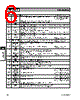
Pin
Function
Description
Interface Schematic
25
PCS LNA
OUT
High-band LNA output (collector). Small external inductance required
for best impedance match to 50
Ω.
26
VCC2
High-band LNA power supply connection. Small series inductance
required.
27
GND2
High-band LNA emitter. Low-inductance ground required.
28
GND2
Same as pin 27.
29
GND2
Same as pin 27.
30
PCS LNA IN High-band LNA input (base). Simple external matching required for
best performance.
31
BAND SEL
Logic input. High selects high-band operation; low selects low-band
operation.
Diode to VCC and Ground.
CMOS logic interface.
32
X2 ENABLE Logic input. High enables LO doubler; low disables LO doubler.
Diode to VCC and Ground.
CMOS logic interface.
Die
Flag
GND
Low inductance ground connection critical to proper operation.


 Portuguese ▼
 English
 Chinese
 German
 Japanese
 Russian
 Korean
 Spanish
 French
 Italian
 Portuguese
 Polish
 Vietnamese
 Indian
 Mexican
 British
 New Zealand