Preliminary
8-38
RF2492
Rev A4 010828
8
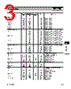
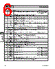
Pin
Function
Description
Interface Schematic
1LO IN
LO input for both bands. Impedance is approximately (120-j25)
Ω.1kΩ shunt resistor (static bleed).
AC coupled to transistor base
(internal DC block).
2
VCC2
Power supply connection for internal LO amplifiers. External low-induc-
tance bypass capacitor between 1nF and 47nF recommended.
3GND
Ground connection.
4IF1+
High-band IF output. Open collector. “Current combiner” IF interface to
1000
Ω SAW filter recommended
2pF internal shunt capacitance.
5IF1-
High-band IF output. Open collector. “Current combiner” IF interface to
1000
Ω SAW filter recommended
2pF internal shunt capacitance.
6BYPASS
Pin requires external bypass capacitor between 1nF and 47nF.
7IF2-
Low-band IF output. Open collector. “Current combiner” IF interface to
1000
Ω SAW filter recommended
2pF internal shunt capacitance.
8IF2+
Low-band IF output. Open collector. “Current combiner” IF interface to
1000
Ω SAW filter recommended
2pF internal shunt capacitance.
9
IF SEL
Logic input. High selects IF1 mixer; low selects IF2 mixer.
Diode to VCC and Ground.
CMOS logic interface.
10
LNA IP SEL Logic input. High selects external LNA current reference (pin 17); low
selects internal LNA current reference.
Diode to VCC and Ground.
CMOS logic interface.
11
CELL LNA
IN
Low-band LNA input (base). Simple external matching required for best
performance.
12
LNA GAIN
SEL
Logic input. High selects maximum LNA gain; low selects minimum
LNA gain.
Diode to VCC and Ground.
CMOS logic interface.
13
VCC1
Power supply for internal references, logic, and mixer preamplifiers.
Internal RF bypass capacitor. External bypass capacitor between 1nF
and 47nF required.
14
MIX GAIN
SEL
Logic input. High selects maximum mixer gain (mixer RF amp on); low
selects minimum mixer gain (mixer RF amp off).
Diode to VCC and Ground.
CMOS logic interface.
15
CELL LNA
OUT
Low-band LNA output (collector). Simple external L-C matching
required.
16
GND
Ground connection. See evaluation board layout.
17
LNA ISET
External current reference for LNA. Resistor to ground sets LNA cur-
rent when Pin 10 is high. 20k
Ω results in approximately 10mA LNA cur-
rent. Higher resistance results in lower current.
18
CELL MIX
IN
Low band mixer RF preamplifier input (base). External L-C network
required for best performance.
19
PCS LO
OUT+
High-band buffered LO output.
Internal DC blocking capacitor.
1k
Ω shunt resistor (static bleed).
20
PCS LO
OUT-
High-band buffered LO output.
Internal DC blocking capacitor.
1k
Ω shunt resistor (static bleed).
21
CELL LO
OUT+
Low-band buffered LO output.
Internal DC blocking capacitor.
1k
Ω shunt resistor (static bleed).
22
CELL LO
OUT-
Low-band buffered LO output.
Internal DC blocking capacitor.
1k
Ω shunt resistor (static bleed).
23
PCS MIX IN High-band mixer RF preamplifier input (base). External L-C network
required for best performance.
24
GND
Ground connection. Keep traces physically short and connect immedi-
ately to ground plane (low-inductance ground required for best perfor-
mance).


 Portuguese ▼
 English
 Chinese
 German
 Japanese
 Russian
 Korean
 Spanish
 French
 Italian
 Portuguese
 Polish
 Vietnamese
 Indian
 Mexican
 British
 New Zealand