|
Os motores de busca de Datasheet de Componentes eletrônicos |
|
|
Os motores de busca de Datasheet de Componentes eletrônicos |
|
LTC1291BCN8 Folha de dados(PDF) 5 Page - Linear Technology |
|
|
|||||||||||||||||||||||||||||
LTC1291BCN8 Folha de dados(HTML) 5 Page - Linear Technology |
|
|
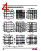
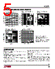
5 / 20 page  5 LTC1291 1291fa CC HARA TERISTICS A TYPICALPERFOR CE DOUT Delay Time vs Temperature Maximum Clock Rate vs Source Resistance Maximum Filter Resistor vs Cycle Time CYCLE TIME ( µs) 10 100 1k 10k 10 1k 10k 1291 G12 1 100 + – +VIN CFILTER ≥1µF RFILTER 100 0.2 0.4 0.6 0.8 1.0 1k 10k 100k 1291 G11 0 VCC = 5V CLK = 1MHz RSOURCE– (Ω) + – +IN –IN +VIN RSOURCE– AMBIENT TEMPERATURE ( °C) –50 0 100 300 400 500 1000 700 –10 30 50 130 1291 G14 200 800 900 600 –30 10 70 90 110 ON CHANNEL OFF CHANNEL GUARANTEED Input Channel Leakage Current vs Temperature Sample-and-Hold Acquisition Time vs Source Resistance * MAXIMUM CLK FREQUENCY REPRESENTS THE CLK FREQUENCY AT WHICH A 0.1LSB SHIFT IN THE ERROR AT ANY CODE TRANSITION FROM ITS 1MHz VALUE IS FIRST DETECTED **MAXIMUM RFILTER REPRESENTS THE FILTER RESISTOR VALUE AT WHICH A 0.1LSB CHANGE IN FULL SCALE ERROR FROM ITS VALUE AT RFILTER = 0Ω IS FIRST DETECTED PI FU CTIO S AMBIENT TEMPERATURE ( °C) –50 150 200 250 50 1291 G10 100 0 –25 0 25 75 125 100 VCC = 5V 50 MSB-FIRST DATA LSB-FIRST DATA RSOURCE+ (Ω) 100 1 10 100 1k 10k 1291 G13 + – VIN RSOURCE+ VCC = 5V TA = 25°C 0V TO 5V INPUT STEP CS (Pin 1): Chip Select Input. A logic low on this input enables the LTC1291. CH0, CH1 (Pins 2, 3): Analog Inputs. These inputs must be free of noise with respect to GND. GND (Pin 4): Analog Ground. GND should be tied directly to an analog ground plane. DIN (Pin 5): Digital Data Input. The multiplexer address is shifted into this input. DOUT (Pin 6): Digital Data Output. The A/D conversion result is shifted out of this output. CLK (Pin 7): Shift Clock. This clock synchronizes the serial data transfer. VCC(VREF) (Pin 8): Positive Supply and Reference Voltage. This pin provides power and defines the span of the A/D converter. This supply must be kept free of noise and ripple by bypassing directly to the analog ground plane. |
|
|
Ligação URL |
| ALLDATASHEET é útil para você? [ DONATE ] |
Sobre Alldatasheet | Publicidade | Contato conosco | Privacy Policy | Link para a ficha técnica | roca de Link | Lista de Fabricantes All Rights Reserved©Alldatasheet.com |
| Russian : Alldatasheetru.com | Korean : Alldatasheet.co.kr | Spanish : Alldatasheet.es | French : Alldatasheet.fr | Italian : Alldatasheetit.com Portuguese : Alldatasheetpt.com | Polish : Alldatasheet.pl | Vietnamese : Alldatasheet.vn Indian : Alldatasheet.in | Mexican : Alldatasheet.com.mx | British : Alldatasheet.co.uk | New Zealand : Alldatasheet.co.nz |
|
Family Site : ic2ic.com |
icmetro.com |
 Portuguese ▼
 English
 Chinese
 German
 Japanese
 Russian
 Korean
 Spanish
 French
 Italian
 Portuguese
 Polish
 Vietnamese
 Indian
 Mexican
 British
 New Zealand