|
Os motores de busca de Datasheet de Componentes eletrônicos |
|
|
Os motores de busca de Datasheet de Componentes eletrônicos |
|
LTC1291BCN8 Folha de dados(PDF) 9 Page - Linear Technology |
|
|
|||||||||||||||||||||||||||||
LTC1291BCN8 Folha de dados(HTML) 9 Page - Linear Technology |
|
|
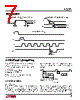
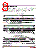
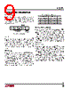
9 / 20 page  9 LTC1291 1291fa Input Data Word The 4-bit data word is clocked into the DIN pin on the rising edge of the clock after chip select goes low and the start bit has been recognized. Further inputs on the DIN pin are then ignored until the next CS cycle. The input word is defined as follows: Start Bit The first “logical one” clocked into the DIN input after CS goes low is the start bit. The start bit initiates the data transfer and all leading zeroes which precede this logical one will be ignored. After the start bit is received, the remaining bits of the input word will be clocked in. Further inputs on the DIN pin are then ignored until the next CS cycle. MUX Address The bits of the input word following the START BIT assign the MUX configuration for the requested conversion. For a given channel selection, the converter will measure the voltage between the two channels indicated by the “+” and “–” signs in the selected row of the following table. In single-ended mode, all input channels are measured with respect to GND. Only the “+” inputs have sample-and- holds. Signals applied at the “–” inputs must not change more than the required accuracy during the conversion. Figure 2. Input Data Word S APPLICATI I FOR ATIO START SGL/ DIFF ODD/ SIGN MSBF MUX ADDRESS MSB-FIRST/ LSB-FIRST POWER SHUTDOWN 1291 F02 PS Multiplexer Channel Selection MUX ADDRESS CHANNEL # SGL/DIFF ODD/SIGN 0 1 GND 10 + – 11 + – 00 + – 01 – + MSB-First/LSB-First (MSBF) The output data of the LTC1291 is programmed for MSB- first or LSB-first sequence using the MSBF bit. When the MSBF bit is a logical one, data will appear on the DOUT line in MSB-first format. Logical zeroes will be filled in indefi- nitely following the last data bit to accommodate longer word lengths required by some microprocessors. When the MSBF bit is a logical zero, LSB-first data will follow the normal MSB-first data on the DOUT line (see Operating Sequence). Power Shutdown The power shutdown feature of the LTC1291 is activated by making the PS bit a logical zero. If CS remains low after the PS bit has been received, a 12-bit DOUT word with all logical ones will be shifted out followed by logical zeroes until CS goes high. Then the DOUT line will go into its high impedance state. The LTC1291 will remain in the shut- down mode until the next CS cycle. There is no warm-up or wait period required after coming out of the power shutdown cycle so a conversion can commence after CS goes low (see Power Shutdown Operating Sequence). |
|
|
Ligação URL |
| ALLDATASHEET é útil para você? [ DONATE ] |
Sobre Alldatasheet | Publicidade | Contato conosco | Privacy Policy | Link para a ficha técnica | roca de Link | Lista de Fabricantes All Rights Reserved©Alldatasheet.com |
| Russian : Alldatasheetru.com | Korean : Alldatasheet.co.kr | Spanish : Alldatasheet.es | French : Alldatasheet.fr | Italian : Alldatasheetit.com Portuguese : Alldatasheetpt.com | Polish : Alldatasheet.pl | Vietnamese : Alldatasheet.vn Indian : Alldatasheet.in | Mexican : Alldatasheet.com.mx | British : Alldatasheet.co.uk | New Zealand : Alldatasheet.co.nz |
|
Family Site : ic2ic.com |
icmetro.com |
 Portuguese ▼
 English
 Chinese
 German
 Japanese
 Russian
 Korean
 Spanish
 French
 Italian
 Portuguese
 Polish
 Vietnamese
 Indian
 Mexican
 British
 New Zealand