|
Os motores de busca de Datasheet de Componentes eletrônicos |
|
|
Os motores de busca de Datasheet de Componentes eletrônicos |
|
ADAR4002ACPZ-R7 Folha de dados(PDF) 8 Page - Analog Devices |
|
|
|||||||||||||||||||||||||||||
ADAR4002ACPZ-R7 Folha de dados(HTML) 8 Page - Analog Devices |
|
|
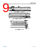
8 / 66 page  Data Sheet ADAR4002 SPECIFICATIONS analog.com Rev. A | 8 of 66 TIMING SPECIFICATIONS V1P2 = 1.2 V, V1P0 = 1.0 V, and TA = 25°C, unless otherwise noted. See Figure 3, Figure 4, Figure 5, and Figure 8 for the supporting timing figures. Table 2. SPI Timing Parameter Min Typ Max Unit Test Conditions/Comments Maximum Clock Rate (1/tCLK_IN) 100 MHz Minimum Clock Period (tCLK_IN) 10 ns Minimum Pulse Width High (tPWH)1 4 ns Minimum Pulse Width Low (tPWL)1 4 ns Minimum Setup Time, DATA_IO to CLK_IN (tDS) 2.5 ns Minimum Hold Time, DATA_IO to CLK_IN (tDH) 1 ns Data Valid, CLK_IN to DATA_O (tDV) 2 ns Setup Time, CSB_CLKO to CLK_IN (tDCS) 5 ns DATA_IO and DATA_O Rise Time (tR) 1 ns Outputs loaded with 80 pF, 10% to 90% Minimum Clock to Update (tCLK_IN-UPDATE) 10 ns Minimum CSB_CLKO to Update (tCSB_CLKO-UPDATE) 10 ns Minimum Update to Update (tUPDATE-UPDATE) 10 ns Minimum Update Pulse width (tUPW) 5 ns RF Settling Time (tRF_SETTLE) 20 ns TDU settling time between TDU code = 0 to TDU code = 127 1 Clock Period = Pulse Width High + Pulse Width Low; however, Minimum Clock Period cannot equal Minimum Pulse Width High + Minimum Pulse Width Low, which allows for the SPI signals that are not 50% duty cycle. The extreme example is if the pulse width high = 4 ns, then the pulse width low = 6 ns, or vice versa. Table 3. Shift Register Mode Timing Parameter Min Typ Max Unit Test Conditions/Comments Maximum Clock Rate (1/tCLK_IN) 100 MHz Minimum Clock Period (tCLK_IN) 10 ns Minimum Pulse Width High (tPWH)1 4 ns Minimum Pulse Width Low (tPWL)1 4 ns Minimum Setup Time, DATA_IO to CLK_IN (tDS) 2.5 ns Minimum Hold Time, DATA_IO to CLK_IN (tDH) 1 ns Data Valid, CLK_IN to DATA_O (tDV) 2 ns DATA_IO, DATA_O Rise Time (tR) 1 ns Outputs loaded with 80 pF, 10% to 90% Minimum Clock to Update (tCLK_IN-UPDATE) 10 ns RF Settling Time (tRF_SETTLE) 20 ns TDU settling time between TDU code = 0 to TDU code = 127 1 Clock Period = Pulse Width High + Pulse Width Low; however, Minimum Clock Period cannot equal Minimum Pulse Width High + Minimum Pulse Width Low, which allows for the SPI signals that are not 50% duty cycle. The extreme example is if the pulse width high = 4 ns, then the pulse width low = 6 ns, or vice versa. TIMING DIAGRAMS Figure 2. SPI Register Timing (MSB First) |
|
Ligação URL |
| ALLDATASHEET é útil para você? [ DONATE ] |
Sobre Alldatasheet | Publicidade | Contato conosco | Privacy Policy | Link para a ficha técnica | roca de Link | Lista de Fabricantes All Rights Reserved©Alldatasheet.com |
| Russian : Alldatasheetru.com | Korean : Alldatasheet.co.kr | Spanish : Alldatasheet.es | French : Alldatasheet.fr | Italian : Alldatasheetit.com Portuguese : Alldatasheetpt.com | Polish : Alldatasheet.pl | Vietnamese : Alldatasheet.vn Indian : Alldatasheet.in | Mexican : Alldatasheet.com.mx | British : Alldatasheet.co.uk | New Zealand : Alldatasheet.co.nz |
|
Family Site : ic2ic.com |
icmetro.com |
 Portuguese ▼
 English
 Chinese
 German
 Japanese
 Russian
 Korean
 Spanish
 French
 Italian
 Portuguese
 Polish
 Vietnamese
 Indian
 Mexican
 British
 New Zealand