|
Os motores de busca de Datasheet de Componentes eletrônicos |
|
|
Os motores de busca de Datasheet de Componentes eletrônicos |
|
AD8132ARZ-R7 Folha de dados(PDF) 22 Page - Analog Devices |
|
|
|||||||||||||||||||||||||||||
AD8132ARZ-R7 Folha de dados(HTML) 22 Page - Analog Devices |
|
|
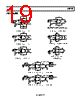
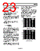
22 / 32 page  AD8132 Rev. F | Page 22 of 32 OTHER β2 = 1 CIRCUITS The preceding simple configuration with β2 = 1 and its gain of 2 is the highest gain circuit that can be made under this condition. Since β1 was equal to 0, only higher β1 values are possible. The circuits with higher values of β1 have gains lower than 2. However, circuits with β1 equal to 1 are not practical because they have no effective input and result in a gain of 0. To increase β1 from 0, it is necessary to add two resistors in a feed- back network. A generalized circuit that has β1 with a value higher than 0 is shown in Figure 69. A couple of different convenient gains that can be created are a gain of 1, when β1 is equal to 1/3, and a gain of 0.5, when β1 equals 0.6. With β2 equal to 1 in these circuits, VOCM serves as the refer- ence voltage that measures the input voltage and the individual output voltages. In general, when VOCM is varied in circuits with unmatched feedback networks, a differential output signal is generated that is proportional to the applied VOCM voltage. VARYING β2 Though the β2 = 1 circuit sets β2 to 1, another class of simple circuits can be made that sets β2 equal to 0. This means that there is no feedback from +OUT to −IN. This class of circuits is very similar to a conventional inverting op amp. However, the AD8132 circuits have an additional output and common- mode input that can be analyzed separately (see Figure 71). With −IN connected to ground, +IN becomes a virtual ground in the sense that the term is used for conventional op amps. Both inputs must maintain the same voltage for equilibrium operation; therefore, if one is set to ground, the other is driven to ground. The input impedance can also be seen to be equal to RG, just as in a conventional op amp. In this case, however, the positive input and negative output are used for the feedback network. Because a conventional op amp does not have a negative output, only its inverting input can be used for the feedback network. The AD8132 is symmetrical, there- fore, the feedback network on either side can be used to produce the same results. Because +IN is a summing junction, by an analogy to conven- tional op amps, the gain from VIN to −OUT is −RF/RG. This holds true regardless of the voltage on VOCM, and since +OUT moves the same amount in the opposite direction from −OUT, the overall gain is −2(RF/RG). VOCM still governs VOUT,cm, so +OUT must be the only output that moves when VOCM is varied. Because VOUT,cm is the average of the two outputs, +OUT must move twice as far and in the same direction as VOCM to create the proper VOUT, cm. Therefore, the gain from VOCM to +OUT must be 2. With β2 equal to 0 in these circuits, the gain can theoretically be set to any value from close to 0 to infinity, just as it can with a conventional op amp in the inverting mode. However, practical real-world limitations and parasitics limit the range of acceptable gain to more modest values. β1 = 0 There is yet another class of circuits where there is no feed- back from −OUT to +IN. This is the case where β1 = 0. The differential amplifier without a resistor described in the Differential Amplifier Without Resistors (High Input Impedance Inverting Amplifier) section meets this condition, but it was presented only with the condition that β2 = 1. Recall that this circuit had a gain equal to 2. If β2 decreases in this circuit from unity, a smaller part of +VOUT is fed back to −IN and the gain increases (see Figure 68). This circuit is very similar to a noninverting op amp configuration, except for the presence of the additional complementary output. Therefore, the overall gain is twice that of a noninverting op amp or 2 × (1 + RF2/RG2) or 2 × (1/β2). Once again, varying VOCM does not affect both outputs in the same way; therefore, in addition to varying VOUT, cm with unity gain, there is also an effect on VOUT, dm by changing VOCM. ESTIMATING THE OUTPUT NOISE VOLTAGE Similar to the case of a conventional op amp, the differential output errors (noise and offset voltages) can be estimated by multiplying the input referred terms, at +IN and −IN, by the circuit noise gain. The noise gain is defined as ⎟ ⎠ ⎞ ⎜ ⎝ ⎛ + = G F N R R G 1 To compute the total output referred noise for the circuit of Figure 64, consideration must be given to the contribution of resistors, RF and RG. See Table 11 for estimated output noise voltage densities at various closed-loop gains. Table 11. Recommended Resistor Values and Noise Performance for Specific Gains Gain RG (Ω) RF (Ω) Bandwidth −3 dB (MHz) Output Noise AD8132 Only (nV/√Hz) Output Noise AD8132 + RG, RF (nV/√Hz) 1 499 499 360 16 17 2 499 1.0 k 160 24.1 26.1 5 499 2.49 k 65 48.4 53.3 10 499 4.99 k 20 88.9 98.6 |
|
Ligação URL |
| ALLDATASHEET é útil para você? [ DONATE ] |
Sobre Alldatasheet | Publicidade | Contato conosco | Privacy Policy | Link para a ficha técnica | roca de Link | Lista de Fabricantes All Rights Reserved©Alldatasheet.com |
| Russian : Alldatasheetru.com | Korean : Alldatasheet.co.kr | Spanish : Alldatasheet.es | French : Alldatasheet.fr | Italian : Alldatasheetit.com Portuguese : Alldatasheetpt.com | Polish : Alldatasheet.pl | Vietnamese : Alldatasheet.vn Indian : Alldatasheet.in | Mexican : Alldatasheet.com.mx | British : Alldatasheet.co.uk | New Zealand : Alldatasheet.co.nz |
|
Family Site : ic2ic.com |
icmetro.com |
 Portuguese ▼
 English
 Chinese
 German
 Japanese
 Russian
 Korean
 Spanish
 French
 Italian
 Portuguese
 Polish
 Vietnamese
 Indian
 Mexican
 British
 New Zealand