|
Os motores de busca de Datasheet de Componentes eletrônicos |
|
|
Os motores de busca de Datasheet de Componentes eletrônicos |
|
AD8132ARZ-R7 Folha de dados(PDF) 21 Page - Analog Devices |
|
|
|||||||||||||||||||||||||||||
AD8132ARZ-R7 Folha de dados(HTML) 21 Page - Analog Devices |
|
|
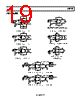
21 / 32 page  AD8132 Rev. F | Page 21 of 32 THEORY OF OPERATION The AD8132 differs from conventional op amps by the external presence of an additional input and output. The additional input, VOCM, controls the output common-mode voltage. The additional output is the analog complement of the single output of a conven- tional op amp. For its operation, the AD8132 uses two feedback loops as compared to the single loop of conventional op amps. Although this provides significant freedom to create various novel circuits, basic op amp theory can still be used to analyze the operation. One of the feedback loops controls the output common-mode voltage, VOUT, cm. Its input is VOCM (Pin 2) and the output is the common-mode, or average voltage, of the two differential outputs (+OUT and −OUT). The gain of this circuit is internally set to unity. When the AD8132 is operating in its linear region, this establishes one of the operational constraints: VOUT, cm = VOCM. The second feedback loop controls the differential operation. Similar to an op amp, the gain and gain shaping of the transfer function can be controlled by adding passive feedback networks. However, only one feedback network is required to close the loop and fully constrain the operation, but depending on the function desired, two feedback networks can be used. This is possible because there are two outputs that are each inverted with respect to the differential inputs. GENERAL USAGE OF THE AD8132 Several assumptions are made here for a first-order analysis; they are the typical assumptions used for the analysis of op amps: • The input bias currents are sufficiently small so they can be neglected. • The output impedances are arbitrarily low. • The open-loop gain is arbitrarily large, and drives the amplifier to a state where the input differential voltage is effectively 0. • Offset voltages are assumed to be 0. Though it is possible to operate the AD8132 with a purely differential input, many of its applications call for a circuit that has a single-ended input with a differential output. For a single-ended-to-differential circuit, the RG of the input that is not driven is tied to a reference voltage. This is ground. Other conditions are discussed in the following sections. In addition, the voltage at VOCM, and therefore VOUT,cm, is assumed to be ground. Figure 67 shows a generalized schematic of such a circuit using an AD8132 with two feedback paths. For each feedback network, a feedback factor can be defined as the fraction of the output signal that is fed back to the opposite sign input. These terms are ( ) F1 G1 G1 R R R β1 + = ( ) F2 G2 G2 R R R β2 + = The feedback factor, β1, is for the side that is driven, and the feedback factor, β2, is for the side that is tied to a reference voltage (ground). Note that each feedback factor can vary anywhere between 0 and 1. A single-ended-to-differential gain equation can be derived (this is true for all values of β1 and β2): ( ) () β2 β1 β1 G + − = 1 2 This expression is not very intuitive, but some further examples can provide better understanding of its implications. One observation that can be made immediately is that a tolerance error in β1 does not have the same effect on gain as the same tolerance error in β2. DIFFERENTIAL AMPLIFIER WITHOUT RESISTORS (HIGH INPUT IMPEDANCE INVERTING AMPLIFIER) The simplest closed-loop circuit that can be made does not require any resistors and is shown in Figure 70. In this circuit, β1 is equal to 0, and β2 is equal to 1. The gain is equal to 2. A more intuitive method to figure the gain is by simple inspection. +OUT is connected to −IN, whose voltage is equal to the voltage at +IN under equilibrium conditions. Thus, +VOUT is equal to VIN, and there is unity gain in this path. Because −OUT has to swing in the opposite direction from +OUT due to the common-mode constraint, its effect doubles the output signal and produces a gain of 2. One useful function that this circuit provides is a high input impedance inverter. If +OUT is ignored, there is a unity-gain, high input impedance amplifier formed from +IN to −OUT. Most traditional op amp inverters have relatively low input impedances, unless they are buffered with another amplifier. VOCM is assumed to be at midsupply. Because there is still the constraint that +VOUT must equal VIN, changing the VOCM voltage does not change +VOUT (equal to VIN). Therefore, the effect of changing VOCM must show up at −OUT. For example, if VOCM is raised by 1 V, then −VOUT must increase by 2 V. This makes VOUT,cm also increase by 1 V, because it is defined as the average of the two differential output voltages. This means that the gain from VOCM to the differential output is 2. |
|
Ligação URL |
| ALLDATASHEET é útil para você? [ DONATE ] |
Sobre Alldatasheet | Publicidade | Contato conosco | Privacy Policy | Link para a ficha técnica | roca de Link | Lista de Fabricantes All Rights Reserved©Alldatasheet.com |
| Russian : Alldatasheetru.com | Korean : Alldatasheet.co.kr | Spanish : Alldatasheet.es | French : Alldatasheet.fr | Italian : Alldatasheetit.com Portuguese : Alldatasheetpt.com | Polish : Alldatasheet.pl | Vietnamese : Alldatasheet.vn Indian : Alldatasheet.in | Mexican : Alldatasheet.com.mx | British : Alldatasheet.co.uk | New Zealand : Alldatasheet.co.nz |
|
Family Site : ic2ic.com |
icmetro.com |
 Portuguese ▼
 English
 Chinese
 German
 Japanese
 Russian
 Korean
 Spanish
 French
 Italian
 Portuguese
 Polish
 Vietnamese
 Indian
 Mexican
 British
 New Zealand