|
Os motores de busca de Datasheet de Componentes eletrônicos |
|
|
Os motores de busca de Datasheet de Componentes eletrônicos |
|
ADP3193 Folha de dados(PDF) 14 Page - Analog Devices |
|
|
|||||||||||||||||||||||||||||
ADP3193 Folha de dados(HTML) 14 Page - Analog Devices |
|
|
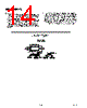
14 / 16 page  REV. A ADP3158/ADP3178 –14– Signal Circuitry 12. The output voltage is sensed and regulated between the GND pin (which connects to the signal ground plane) and the CS– pin. The output current is sensed (as a voltage) and regulated between the CS– pin and the CS+ pin. In order to avoid differential mode noise pickup in those sensed signals, their loop areas should be small. Thus the CS– trace should be routed atop the signal ground plane, and the CS+ and CS– traces should be routed as a closely coupled pair (CS+ should be over the signal ground plane as well). OUTLINE DIMENSIONS Dimensions shown in inches and (mm). 16-Lead SOIC (R-16A/SO-16) 16 9 8 1 0.2440 (6.20) 0.2284 (5.80) 0.1574 (4.00) 0.1497 (3.80) PIN 1 0.3937 (10.00) 0.3859 (9.80) 0.050 (1.27) BSC SEATING PLANE 0.0098 (0.25) 0.0040 (0.10) 0.0192 (0.49) 0.0138 (0.35) 0.0688 (1.75) 0.0532 (1.35) 8 0 0.0196 (0.50) 0.0099 (0.25) 45 0.0500 (1.27) 0.0160 (0.41) 0.0099 (0.25) 0.0075 (0.19) 13. The CS+ and CS– traces should be Kelvin-connected to the current sense resistor so that the additional voltage drop due to current flow on the PCB at the current sense resistor connections does not affect the sensed voltage. It is desir- able to have the controller IC close to the output capacitor bank and not in the output power path, so that any voltage drop between the output capacitors and the GND pin is minimized, and voltage regulation is not compromised. |
|
|
Ligação URL |
| ALLDATASHEET é útil para você? [ DONATE ] |
Sobre Alldatasheet | Publicidade | Contato conosco | Privacy Policy | Link para a ficha técnica | roca de Link | Lista de Fabricantes All Rights Reserved©Alldatasheet.com |
| Russian : Alldatasheetru.com | Korean : Alldatasheet.co.kr | Spanish : Alldatasheet.es | French : Alldatasheet.fr | Italian : Alldatasheetit.com Portuguese : Alldatasheetpt.com | Polish : Alldatasheet.pl | Vietnamese : Alldatasheet.vn Indian : Alldatasheet.in | Mexican : Alldatasheet.com.mx | British : Alldatasheet.co.uk | New Zealand : Alldatasheet.co.nz |
|
Family Site : ic2ic.com |
icmetro.com |
 Portuguese ▼
 English
 Chinese
 German
 Japanese
 Russian
 Korean
 Spanish
 French
 Italian
 Portuguese
 Polish
 Vietnamese
 Indian
 Mexican
 British
 New Zealand