|
Os motores de busca de Datasheet de Componentes eletrônicos |
|
|
Os motores de busca de Datasheet de Componentes eletrônicos |
|
LT8636 Folha de dados(PDF) 6 Page - Analog Devices |
|
|
|||||||||||||||||||||||||||||
LT8636 Folha de dados(HTML) 6 Page - Analog Devices |
|
|
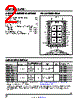
6 / 40 page  LT8698S/LT8698S-1 6 Rev. A For more information www.analog.com SYMBOL PARAMETER CONDITIONS MIN TYP MAX UNITS 1A CHARGER PROFILE HD+ Voltage VBUS/ISN = 5V 1.94 2.00 2.06 V HD+ Output Resistance 30 kΩ HD– Voltage VBUS/ISN = 5V 2.60 2.68 2.76 V HD– Output Resistance 23 kΩ 2A CHARGER PROFILE HD+, HD– Voltage VBUS/ISN = 5V 1.2 1.25 1.35 V HD+, HD– Output Resistance 7.5 kΩ ELECTRICAL CHARACTERISTICS The l denotes the specifications which apply over the full operating temperature range, otherwise specifications are at TA = 25°C. (Note 2) Note 1: Stresses beyond those listed under Absolute Maximum Ratings may cause permanent damage to the device. Exposure to any Absolute Maximum Rating condition for extended periods may affect device reliability and lifetime. Note 2: The LT8698SE and LT8698SE-1 are guaranteed to meet performance specifications from 0˚C to 125°C junction temperature. Specifications over the −40°C to 125°C operating junction temperature range are assured by design, characterization and correlation with statistical process controls. The LT8698SJ and LT8698SJ-1 are guaranteed over the full −40°C to 150°C operating temperature range. High junction temperatures degrade operating lifetime. Operating lifetime is de-rated at junction temperatures greater than 125°C. The junction temperature (TJ in °C) is calculated from the ambient temperature (TA in °C) and power dissipation (PD in Watts) according to the formula: TJ = TA + (PD • θJA) where θJA (in °C/W) is the package thermal impedance. Note 3: This IC includes overtemperature protection that is intended to protect the device during overload conditions. Junction temperature will exceed 150°C when overtemperature protection is active. Continuous operation above the specified maximum operating junction temperature will reduce lifetime. Note 4: DUT configured in closed loop test circuit similar to page 36 CDP charger application circuit. Note 5: Parameter not tested in production. Note 6: θ values are determined by simulation per JESD51 conditions, except θJA value is determined by simulation with demo board. See Applications Information section for more information on PCB layout considerations and example thermal data. |
|
Ligação URL |
| ALLDATASHEET é útil para você? [ DONATE ] |
Sobre Alldatasheet | Publicidade | Contato conosco | Privacy Policy | Link para a ficha técnica | roca de Link | Lista de Fabricantes All Rights Reserved©Alldatasheet.com |
| Russian : Alldatasheetru.com | Korean : Alldatasheet.co.kr | Spanish : Alldatasheet.es | French : Alldatasheet.fr | Italian : Alldatasheetit.com Portuguese : Alldatasheetpt.com | Polish : Alldatasheet.pl | Vietnamese : Alldatasheet.vn Indian : Alldatasheet.in | Mexican : Alldatasheet.com.mx | British : Alldatasheet.co.uk | New Zealand : Alldatasheet.co.nz |
|
Family Site : ic2ic.com |
icmetro.com |
 Portuguese ▼
 English
 Chinese
 German
 Japanese
 Russian
 Korean
 Spanish
 French
 Italian
 Portuguese
 Polish
 Vietnamese
 Indian
 Mexican
 British
 New Zealand