|
Os motores de busca de Datasheet de Componentes eletrônicos |
|
|
Os motores de busca de Datasheet de Componentes eletrônicos |
|
ADP3158JR Folha de dados(PDF) 3 Page - Analog Devices |
|
|
|||||||||||||||||||||||||||||
ADP3158JR Folha de dados(HTML) 3 Page - Analog Devices |
|
|
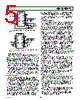
3 / 16 page  REV. A ADP3158/ADP3178 –3– ABSOLUTE MAXIMUM RATINGS * VCC . . . . . . . . . . . . . . . . . . . . . . . . . . . . . . . –0.3 V to +15 V DRVH, DRVL, LRDRV1, LRDRV2 . . . . . –0.3 V to VCC + 0.3 V All Other Inputs and Outputs . . . . . . . . . . . . –0.3 V to +10 V Operating Ambient Temperature Range . . . . . . . 0 °C to 70°C Operating Junction Temperature . . . . . . . . . . . . . . . . . 125 °C Storage Temperature Range . . . . . . . . . . . . –65 °C to +150°C θ JA Two-Layer Board . . . . . . . . . . . . . . . . . . . . . . . . . 125 °C/W Four-Layer Board . . . . . . . . . . . . . . . . . . . . . . . . . . 81 °C/W Lead Temperature (Soldering, 10 sec) . . . . . . . . . . . . 300 °C Vapor Phase (60 sec) . . . . . . . . . . . . . . . . . . . . . . . . . . 215 °C Infrared (15 sec) . . . . . . . . . . . . . . . . . . . . . . . . . . . . . 220 °C *This is a stress rating only; operation beyond these limits can cause the device to be permanently damaged. Unless otherwise specified, all voltages are referenced to GND. PIN CONFIGURATION TOP VIEW (Not to Scale) 16 15 14 13 12 11 10 9 1 2 3 4 5 6 7 8 VID0 VID1 VID2 VID3 LRFB1 LRDRV1 CS– CS+ GND DRVH DRVL VCC LRFB2 LRDRV2 COMP CT ADP3158/ ADP3178 PIN FUNCTION DESCRIPTIONS Pin Mnemonic Function 1–4 VID0–VID3 Voltage Identification DAC Inputs. These pins are pulled up to an internal reference, providing a Logic 1 if left open. The DAC output programs the CS– regulation voltage from 1.3 V to 2.05 V. 5, 12 LRFB1, Feedback connections for the linear LRFB2 regulator controllers. 6, 11 LRDRV1, Gate drives for the respective linear LRDRV2 regulator N-channel MOSFETs. 7 CS– Current Sense Negative Node. Negative input for the current comparator. This pin also connects to the internal error ampli- fier that senses the output voltage. 8 CS+ Current Sense Positive Node. Positive input for the current comparator. The output current is sensed as a voltage at this pin with respect to CS–. 9 CT External capacitor connected from CT to ground sets the Off-time of the device. 10 COMP Error Amplifier Output and Compensation Point. The voltage at this output programs the output current control level between CS+ and CS–. 13 VCC Supply Voltage for the device. 14 DRVL Low-Side MOSFET Drive. Gate drive for the synchronous rectifier N-channel MOSFET. The voltage at DRVL swings from GND to VCC. 15 DRVH High-Side MOSFET Drive. Gate drive for the buck switch N-channel MOSFET. The voltage at DRVH swings from GND to VCC. 16 GND Ground Reference. GND should have a low impedance path to the source of the synchronous MOSFET. ORDERING GUIDE Temperature LDO Package Package Model Range Voltage Description Option ADP3158JR 0 °C to 70°C 2.5 V, 1.8 V SO = Small Outline Package R-16A (SO-16) ADP3178JR 0 °C to 70°C Adjustable SO = Small Outline Package R-16A (SO-16) CAUTION ESD (electrostatic discharge) sensitive device. Electrostatic charges as high as 4000 V readily accumulate on the human body and test equipment and can discharge without detection. Although the ADP3158/ADP3178 feature proprietary ESD protection circuitry, permanent damage may occur on devices subjected to high-energy electrostatic discharges. Therefore, proper ESD precautions are recommended to avoid performance degradation or loss of functionality. WARNING! ESD SENSITIVE DEVICE |
|
|
Ligação URL |
| ALLDATASHEET é útil para você? [ DONATE ] |
Sobre Alldatasheet | Publicidade | Contato conosco | Privacy Policy | Link para a ficha técnica | roca de Link | Lista de Fabricantes All Rights Reserved©Alldatasheet.com |
| Russian : Alldatasheetru.com | Korean : Alldatasheet.co.kr | Spanish : Alldatasheet.es | French : Alldatasheet.fr | Italian : Alldatasheetit.com Portuguese : Alldatasheetpt.com | Polish : Alldatasheet.pl | Vietnamese : Alldatasheet.vn Indian : Alldatasheet.in | Mexican : Alldatasheet.com.mx | British : Alldatasheet.co.uk | New Zealand : Alldatasheet.co.nz |
|
Family Site : ic2ic.com |
icmetro.com |
 Portuguese ▼
 English
 Chinese
 German
 Japanese
 Russian
 Korean
 Spanish
 French
 Italian
 Portuguese
 Polish
 Vietnamese
 Indian
 Mexican
 British
 New Zealand