|
Os motores de busca de Datasheet de Componentes eletrônicos |
|
|
Os motores de busca de Datasheet de Componentes eletrônicos |
|
ADP3158JR Folha de dados(PDF) 13 Page - Analog Devices |
|
|
|||||||||||||||||||||||||||||
ADP3158JR Folha de dados(HTML) 13 Page - Analog Devices |
|
|
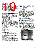
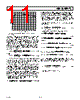
13 / 16 page  REV. A ADP3158/ADP3178 –13– LAYOUT AND COMPONENT PLACEMENT GUIDELINES The following guidelines are recommended for optimal perfor- mance of a switching regulator in a PC system: General Recommendations 1. For best results, a four-layer PCB is recommended. This should allow the needed versatility for control circuitry interconnections with optimal placement, a signal ground plane, power planes for both power ground and the input power (e.g., 5 V), and wide interconnection traces in the rest of the power delivery current paths. 2. Whenever high currents must be routed between PCB layers, vias should be used liberally to create several parallel current paths so that the resistance and inductance intro- duced by these current paths is minimized and the via current rating is not exceeded. 3. If critical signal lines (including the voltage and current sense lines of the controller IC) must cross through power circuitry, it is best if a ground plane can be interposed between those signal lines and the traces of the power circuitry. This serves as a shield to minimize noise injec- tion into the signals at the cost of making signal ground a bit noisier. 4. The GND pin should connect first to a ceramic bypass capacitor (on the VCC pin) and then into the power ground plane. However, the ground plane should not extend under other signal components, including the controller IC itself. 5. The output capacitors should also be connected as closely as possible to the load (or connector) that receives the power (e.g., a microprocessor core). If the load is distributed, the capacitors should also be distributed, and generally in proportion to where the load tends to be more dynamic. It is also advised to keep the planar interconnection path short (i.e., have input and output capacitors close together). 6. Absolutely avoid crossing any signal lines over the switching power path loop, described below. Power Circuitry 7. The switching power path should be routed on the PCB to encompass the smallest possible area in order to minimize radiated switching noise energy (i.e., EMI). Failure to take proper precaution often results in EMI problems for the entire PC system as well as noise-related operational prob- lems in the power converter control circuitry. The switching power path is the loop formed by the current path through the input capacitors, the two FETs, and the power Schottky diode, if used, including all interconnecting PCB traces and planes. The use of short and wide interconnection traces is especially critical in this path for two reasons: it minimizes the inductance in the switching loop, which can cause high- energy ringing, and it accommodates the high current demand with minimal voltage loss. 8. A power Schottky diode (1 ~ 2 A dc rating) placed from the lower MOSFET’s source (anode) to drain (cathode) will help to minimize switching power dissipation in the upper MOSFET. In the bñôÖÑx of an effective Schottky diode, this dissipation occurs through the following sequence of switching events. The lower MOSFET turns off in advance of the upper MOSFET turning on (necessary to prevent cross-conduction). The circulating current in the power converter, no longer finding a path for current through the channel of the lower MOSFET, draws current through the inherent body-drain diode of the MOSFET. The upper MOSFET turns on, and the reverse recovery characteristic of the lower MOSFET’s body-drain diode prevents the drain voltage from being pulled high quickly. The upper MOSFET then conducts very large current while it momentarily has a high voltage forced across it, which translates into added power dissipation in the upper MOSFET. The Schottky diode minimizes this problem by carrying a majority of the circu- lating current when the lower MOSFET is turned off, and by virtue of its essentially nonexistent reverse recovery time. 9. Whenever a power-dissipating component (e.g., a power MOSFET) is soldered to a PCB, the liberal use of vias, both directly on the mounting pad and immediately sur- rounding it, is recommended. Two important reasons for this are: improved current rating through the vias (if it is a current path), and improved thermal performance—espe- cially if the vias extend to the opposite side of the PCB where a plane can more readily transfer the heat to the air. 10. The output power path, though not as critical as the switch- ing power path, should also be routed to encompass a small area. The output power path is formed by the current path through the inductor, the current sensing resistor, the out- put capacitors, and back to the input capacitors. 11. For best EMI containment, the ground plane should extend fully under all the power components. These are: the input capacitors, the power MOSFETs and Schottky diode, the inductor, the current sense resistor, any snubbing elements that might be added to dampen ringing, and the output capacitors. |
|
|
Ligação URL |
| ALLDATASHEET é útil para você? [ DONATE ] |
Sobre Alldatasheet | Publicidade | Contato conosco | Privacy Policy | Link para a ficha técnica | roca de Link | Lista de Fabricantes All Rights Reserved©Alldatasheet.com |
| Russian : Alldatasheetru.com | Korean : Alldatasheet.co.kr | Spanish : Alldatasheet.es | French : Alldatasheet.fr | Italian : Alldatasheetit.com Portuguese : Alldatasheetpt.com | Polish : Alldatasheet.pl | Vietnamese : Alldatasheet.vn Indian : Alldatasheet.in | Mexican : Alldatasheet.com.mx | British : Alldatasheet.co.uk | New Zealand : Alldatasheet.co.nz |
|
Family Site : ic2ic.com |
icmetro.com |
 Portuguese ▼
 English
 Chinese
 German
 Japanese
 Russian
 Korean
 Spanish
 French
 Italian
 Portuguese
 Polish
 Vietnamese
 Indian
 Mexican
 British
 New Zealand