|
Os motores de busca de Datasheet de Componentes eletrônicos |
|
|
Os motores de busca de Datasheet de Componentes eletrônicos |
|
ADP3158JR Folha de dados(PDF) 11 Page - Analog Devices |
|
|
|||||||||||||||||||||||||||||
ADP3158JR Folha de dados(HTML) 11 Page - Analog Devices |
|
|
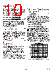
11 / 16 page  REV. A ADP3158/ADP3178 –11– 0 0 2 OUTPUT CURRENT – A 10 20 30 40 50 60 70 80 90 100 46 8 10 12 14 16 18 20 Figure 5. Efficiency vs. Load Current of the Circuit of Figure 3 To correctly implement active voltage positioning, the low fre- quency output impedance (i.e., the output resistance) of the converter should be made equal to the maximum ESR of the output capacitor array. This can be achieved by having a single- pole roll-off of the voltage gain of the gm error amplifier, where the pole frequency coincides with the ESR zero of the output capacitor. A gain with single-pole roll-off requires that the gm amplifier output pin be terminated by the parallel combination of a resistor and capacitor. The required resistor value can be calculated from the equation: R RR RR Mk Mk k COMP OGM TOTAL OGM TOTAL = × = Ω× Ω ΩΩ =Ω – . – . . 19 1 19 1 92 (24) where: R nR gR m mmho m k TOTAL I SENSE m E MAX = × × = ×Ω ×Ω =Ω () . . 25 4 22 5 91 (25) In Equations 24 and 25, ROGM is the internal resistance of the gm amplifier, nI is the division ratio from the output voltage to signal of the gm amplifier to the PWM comparator, and gm is the transconductance of the gm amplifier itself. Although a single termination resistor equal to RCOMP would yield the proper voltage positioning gain, the dc biasing of that resistor would determine how the regulation band is centered (i.e., offset). Note that sometimes the specified regulation band is asymmetrical with respect to the nominal VID voltage. With the ADP3158 and ADP3178, the offset is already considered part of the design procedure—no special provision is required. To accomplish the dc biasing, it is simplest to use two resistors to terminate the gm amplifier output, with the lower resistor (RB) tied to ground and the upper resistor (RA) to the 12 V supply of the IC. The values of these resistors can be calculated using: R V gV K V mmho mV k A DIV m OUT OS = ×+ = ×+ × =Ω () .( . ) . () – 12 22 22 47 10 79 1 2 (26) where K is a constant determined by internal characteristics of the ADP3158 and ADP3178, peak-to-peak inductor current ripple (IRIPPLE), and the current sampling resistor (RSENSE). K can be calculated using Equations 28 and 29. VDIV is the resistor divider supply voltage (e.g., the recommended 12 V supply) and VOUT(OS) is the output voltage offset from the nominal VID-programmed value under no load condition. This offset is given by Equation 30. The closest 1% value for RA is 78.7 k Ω. This value is then used to solve for RB: R RR RR kk kk k B A COMP A COMP = × = Ω× Ω ΩΩ =Ω – .. . – . . 78 7 9 2 78 7 9 2 10 4 (27) The nearest 1% value of 10.5 k Ω was chosen for R B. K I Rn gR V gR V gR K Am mmho k mmho k V mmho k L RIPPLE SENSE I m TOTAL GNL m TOTAL CC m OGM =× × × + ×× =× Ω× ×Ω + ×Ω − ×× Ω =× () – () – . .. . .. . . 22 38 2 425 22 91 1 174 22 91 12 2 2 2 130 47 10 2 VV V RI Vk VmV mA VmV OUT OS OUT MAX VID E MAX L RIPPLE VID VID OUT OS () ( ) () ( ) () – . . =− ()− × −× =− Ω× −× × = 2 40 53 8 2 17 5 10 22 3 Finally, the compensating capacitance is determined from the equality of the pole frequency of the error amplifier gain and the zero frequency of the impedance of the output capacitor: C C ESR R mF m k nF OC OUT TOTAL = × = ×Ω Ω = 54 8 91 26 . . . (31) The closest standard value for COC is 2.7 nF. (28) VV IR n VV L tR n VV Am V V H ns m V GNL GNL L RIPPLE SENSE I IN VID D SENSE I GNL =+ ×× − − ×× × =+ ×Ω × − µ ×× Ω × = 0 2 1 38 4 25 2 51 7 15 75 4 25 1 174 () . – . . . (29) (30) |
|
|
Ligação URL |
| ALLDATASHEET é útil para você? [ DONATE ] |
Sobre Alldatasheet | Publicidade | Contato conosco | Privacy Policy | Link para a ficha técnica | roca de Link | Lista de Fabricantes All Rights Reserved©Alldatasheet.com |
| Russian : Alldatasheetru.com | Korean : Alldatasheet.co.kr | Spanish : Alldatasheet.es | French : Alldatasheet.fr | Italian : Alldatasheetit.com Portuguese : Alldatasheetpt.com | Polish : Alldatasheet.pl | Vietnamese : Alldatasheet.vn Indian : Alldatasheet.in | Mexican : Alldatasheet.com.mx | British : Alldatasheet.co.uk | New Zealand : Alldatasheet.co.nz |
|
Family Site : ic2ic.com |
icmetro.com |
 Portuguese ▼
 English
 Chinese
 German
 Japanese
 Russian
 Korean
 Spanish
 French
 Italian
 Portuguese
 Polish
 Vietnamese
 Indian
 Mexican
 British
 New Zealand