|
Os motores de busca de Datasheet de Componentes eletrônicos |
|
|
Os motores de busca de Datasheet de Componentes eletrônicos |
|
4052 Folha de dados(PDF) 8 Page - Unisonic Technologies |
|
|
|||||||||||||||||||||||||||||
4052 Folha de dados(HTML) 8 Page - Unisonic Technologies |
|
|
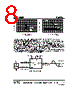
8 / 9 page  UTC 4052 CMOS UTC UNISONIC TECHNOLOGIES CO., LTD. 8 QW-R502-013,A 700 0 300 500 600 -10 Vin,INPUT VOLTAGE (VOLTS) -8.0 0 0.2 6.0 4.0 400 100 200 -6.0 -4.0 -2.0 10 8.0 Figure12.VDD=2.5V,VEE=-2.5V TA=125℃ 25℃ -55℃ 350 0 150 250 300 -10 Vin, INPUT VOLTAGE (VOLTS) -8.0 0 0.2 6.0 4.0 200 50 100 -6.0 -4.0 -2.0 10 8.0 Figure13 Comparison at 25℃,VDD=-VEE TA=25℃ VDD=2.5V 5.0V 7.5V Figure A illustrates use of the on–chip level converter detailed in Figures 2. The 0 ~ 5 V Digital Control signal is used to directly control a 9 Vp–p analog signal. The digital control logic levels are determined by VDD and VSS. The VDD voltage is the logic high voltage; the VSS voltage is logic low. For the example, VDD = + 5 V = logic high at the control inputs; VSS = GND = 0 V = logic low. The maximum analog signal level is determined by VDD and VEE. The VDD voltage determines the maximum recommended peak above VSS. The VEE voltage determines the maximum swing below VSS. For the example, VDD – VSS = 5 V maximum swing above VSS; VSS – VEE = 5 V maximum swing below VSS. The example shows a ± 4.5 V signal which allows a 1/2 volt margin at each peak. If voltage transients above VDD and/or below VEE are anticipated on the analog channels, external diodes (Dx) are recommended as shown in Figure B. These diodes should be small signal types able to absorb the maximum anticipated current surges during clipping. The absolute maximum potential difference between VDD and VEE is 18.0 V. Most parameters are specified up to 15 V which is the recommended maximum difference between VDD and VEE. Balanced supplies are not required. However, VSS must be greater than or equal to VEE. For example, VDD = + 10 V, VSS = + 5 V, and VEE – 3 V is acceptable. See the Table below. EXTERNAL CMOS DIGITAL CIRCUITRY 0 ~ 5V DIGITAL CONTROL SIGNALS ANALOG SIGNAL 9 Vp-p SWITCH I/O INHIBIT, A,B,C COMMON O/I VDD Vss VEE +5V -5V ANALOG SIGNAL 9 Vp-p -4.5V +4.5V GND +5V Figure A. Application Example 4052 |
|
|
Ligação URL |
| ALLDATASHEET é útil para você? [ DONATE ] |
Sobre Alldatasheet | Publicidade | Contato conosco | Privacy Policy | Link para a ficha técnica | roca de Link | Lista de Fabricantes All Rights Reserved©Alldatasheet.com |
| Russian : Alldatasheetru.com | Korean : Alldatasheet.co.kr | Spanish : Alldatasheet.es | French : Alldatasheet.fr | Italian : Alldatasheetit.com Portuguese : Alldatasheetpt.com | Polish : Alldatasheet.pl | Vietnamese : Alldatasheet.vn Indian : Alldatasheet.in | Mexican : Alldatasheet.com.mx | British : Alldatasheet.co.uk | New Zealand : Alldatasheet.co.nz |
|
Family Site : ic2ic.com |
icmetro.com |
 Portuguese ▼
 English
 Chinese
 German
 Japanese
 Russian
 Korean
 Spanish
 French
 Italian
 Portuguese
 Polish
 Vietnamese
 Indian
 Mexican
 British
 New Zealand