 |
Os motores de busca de Datasheet de Componentes eletrônicos |
|
|
Os motores de busca de Datasheet de Componentes eletrônicos |
|
The question interval is too short.
Please try again in a few seconds.

Hello, Please ask a question about ADP151 Datasheet
# Example questions:
➢ The adp151 has an internal pull-down resistor on the en pin. what does this feature allow, and why is it beneficial?
➢ What is a key benefit of the adp151 for battery-powered applications?
➢ The documentation mentions several performance characteristics being tested at a specific input voltage (5v) and output current (1ma). what is the primary purpose of these tests?
| Part No. | ADP151 |
| Manufacturer | AD |
| Size | 1Mb |
| Pages | 23 pages |
| Description | Ultralow Noise, 200 mA, CMOS Linear Regulator |








1. General Description & Features:
️· What it is: A low-noise, low-quiescent current (low quiescent current = efficient), Linear Regulator (LDO). LDOs are voltage regulators that reduce voltage drop linearly, unlike switching regulators.
️· Input Voltage: 2.2V to 5.5V.
️· Output Current: Up to 200mA.
️· Low Noise: Designed for sensitive analog and RF applications; doesn't *require* a bypass capacitor for noise reduction.
️· Efficiency: Very efficient, with low quiescent current (265 μA typical at full load).
️· Shutdown Current: Very low when disabled (typically 0.2 μA) – good for battery-powered devices.
️· Output Voltages: Available in 16 different output voltage options ranging from 1.1V to 3.3V.
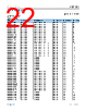
️· Package Options: Available in TSOT, WLCSP and LFCSP packages.
2. Key Specifications (Typical Values are Listed):
️· Quiescent Current (Iq): 265 μA at full load.
️· Shutdown Current: 0.2 μA.
️· Output Voltage Accuracy: See datasheet for specific voltage options and tolerances.
️· Dropout Voltage: The minimum voltage difference needed between input and output to maintain regulation. (See graphs in the datasheet)
️· Noise: Very low output noise (See graphs in the datasheet).
️· Power Supply Rejection Ratio (PSRR): A measure of how well the regulator rejects noise on the input supply voltage. (See graphs in the datasheet).
️· Load Transient Response: How quickly the regulator responds to changes in load current (See graphs in the datasheet).
3. How it Works (Theory of Operation):
️· Architecture: Uses a reference voltage, error amplifier, voltage divider, and a PMOS pass transistor.
️· Regulation: The error amplifier compares the output voltage (feedback) with a reference voltage. It adjusts the PMOS pass transistor to maintain a stable output voltage.
️· Enable (EN) Pin:
- Connect to VIN for automatic startup.
- Pull low to disable the output voltage (VOUT).
- Internal pull-down resistor keeps the EN pin low if left unconnected.
4. Package and Pin Descriptions:
️· Pin 1 (TSOT): Regulator Input (VIN). Requires a 1 µF or greater capacitor connected to ground.
️· Pin 2 (TSOT): Ground (GND).
️· Pin 3 (TSOT): Enable Input (EN).
️· Pin 3 (WLCSP): Enable Input (EN).
️· Pin 3 (LFCSP): Enable Input (EN).
️· Pin 5 (TSOT): Regulated Output Voltage (VOUT). Requires a 1 µF or greater capacitor connected to ground.
️· Pin 1 (WLCSP): Regulated Output Voltage (VOUT).
️· Pin 1 (LFCSP): Regulated Output Voltage (VOUT).
️· EPAD (LFCSP): Exposed Pad - *Must be connected to ground* for optimal thermal performance.
5. Important Graphs and Figures:
The datasheet contains many graphs that are crucial for proper application:
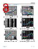
️· Output Voltage vs. Junction Temperature: Shows how the output voltage changes with temperature.
️· Output Voltage vs. Load Current: Shows how the output voltage changes with load.
️· Ground Current vs. Input Voltage: Shows how the ground current changes with input voltage.
️· Dropout Voltage vs. Load Current: Shows how the dropout voltage changes with load.
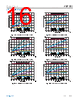
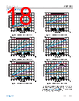
️· PSRR vs. Frequency: Critical for understanding noise performance.
️· Load Transient Response: Shows how quickly the regulator responds to changes in current demand.
️· Output Noise vs. Frequency: Shows the output noise spectrum.
️· Block Diagram: Illustrates the internal architecture.
---
CRITICAL NOTES & DISCLAIMERS:
️· This is a Datasheet: This document is a *datasheet*, not a tutorial. It assumes a basic understanding of electronics and voltage regulation.
️· Typical Values: The values given in the datasheet are *typical* values. Actual performance will vary depending on operating conditions (temperature, load, input voltage).
️· Application Circuits: The datasheet *does not* provide complete application circuits. You are responsible for designing and testing the circuit properly.
️· Capacitor Requirements: The datasheet specifies the need for capacitors on the input (VIN to GND) and output (VOUT to GND). These capacitors are *essential* for stability and proper operation. Use the recommended values.
1. General Description & Features:
️· What it is: A low-noise, low-quiescent current (low quiescent current = efficient), Linear Regulator (LDO). LDOs are voltage regulators that reduce voltage drop linearly, unlike switching regulators.
️· Input Voltage: 2.2V to 5.5V.
️· Output Current: Up to 200mA.
️· Low Noise: Designed for sensitive analog and RF applications; doesn't *require* a bypass capacitor for noise reduction.
️· Efficiency: Very efficient, with low quiescent current (265 μA typical at full load).
️· Shutdown Current: Very low when disabled (typically 0.2 μA) – good for battery-powered devices.
️· Output Voltages: Available in 16 different output voltage options ranging from 1.1V to 3.3V.
️· Package Options: Available in TSOT, WLCSP and LFCSP packages.
2. Key Specifications (Typical Values are Listed):
️· Quiescent Current (Iq): 265 μA at full load.
️· Shutdown Current: 0.2 μA.
️· Output Voltage Accuracy: See datasheet for specific voltage options and tolerances.
️· Dropout Voltage: The minimum voltage difference needed between input and output to maintain regulation. (See graphs in the datasheet)
️· Noise: Very low output noise (See graphs in the datasheet).
️· Power Supply Rejection Ratio (PSRR): A measure of how well the regulator rejects noise on the input supply voltage. (See graphs in the datasheet).
️· Load Transient Response: How quickly the regulator responds to changes in load current (See graphs in the datasheet).
3. How it Works (Theory of Operation):
️· Architecture: Uses a reference voltage, error amplifier, voltage divider, and a PMOS pass transistor.
️· Regulation: The error amplifier compares the output voltage (feedback) with a reference voltage. It adjusts the PMOS pass transistor to maintain a stable output voltage.
️· Enable (EN) Pin:
- Connect to VIN for automatic startup.
- Pull low to disable the output voltage (VOUT).
- Internal pull-down resistor keeps the EN pin low if left unconnected.
4. Package and Pin Descriptions:
️· Pin 1 (TSOT): Regulator Input (VIN). Requires a 1 µF or greater capacitor connected to ground.
️· Pin 2 (TSOT): Ground (GND).
️· Pin 3 (TSOT): Enable Input (EN).
️· Pin 3 (WLCSP): Enable Input (EN).
️· Pin 3 (LFCSP): Enable Input (EN).
️· Pin 5 (TSOT): Regulated Output Voltage (VOUT). Requires a 1 µF or greater capacitor connected to ground.
️· Pin 1 (WLCSP): Regulated Output Voltage (VOUT).
️· Pin 1 (LFCSP): Regulated Output Voltage (VOUT).
️· EPAD (LFCSP): Exposed Pad - *Must be connected to ground* for optimal thermal performance.
5. Important Graphs and Figures:
The datasheet contains many graphs that are crucial for proper application:
️· Output Voltage vs. Junction Temperature: Shows how the output voltage changes with temperature.
️· Output Voltage vs. Load Current: Shows how the output voltage changes with load.
️· Ground Current vs. Input Voltage: Shows how the ground current changes with input voltage.
️· Dropout Voltage vs. Load Current: Shows how the dropout voltage changes with load.
️· PSRR vs. Frequency: Critical for understanding noise performance.
️· Load Transient Response: Shows how quickly the regulator responds to changes in current demand.
️· Output Noise vs. Frequency: Shows the output noise spectrum.
️· Block Diagram: Illustrates the internal architecture.
---
CRITICAL NOTES & DISCLAIMERS:
️· This is a Datasheet: This document is a *datasheet*, not a tutorial. It assumes a basic understanding of electronics and voltage regulation.
️· Typical Values: The values given in the datasheet are *typical* values. Actual performance will vary depending on operating conditions (temperature, load, input voltage).
️· Application Circuits: The datasheet *does not* provide complete application circuits. You are responsible for designing and testing the circuit properly.
️· Capacitor Requirements: The datasheet specifies the need for capacitors on the input (VIN to GND) and output (VOUT to GND). These capacitors are *essential* for stability and proper operation. Use the recommended values.
| Part No. | ADP151 |
| Manufacturer | AD |
| Size | 1Mb |
| Pages | 23 pages |
| Description | Ultralow Noise, 200 mA, CMOS Linear Regulator |
| ALLDATASHEET é útil para você? [ DONATE ] |
Sobre Alldatasheet | Publicidade | Contato conosco | Privacy Policy | Link para a ficha técnica | roca de Link | Lista de Fabricantes All Rights Reserved©Alldatasheet.com |
| Russian : Alldatasheetru.com | Korean : Alldatasheet.co.kr | Spanish : Alldatasheet.es | French : Alldatasheet.fr | Italian : Alldatasheetit.com Portuguese : Alldatasheetpt.com | Polish : Alldatasheet.pl | Vietnamese : Alldatasheet.vn Indian : Alldatasheet.in | Mexican : Alldatasheet.com.mx | British : Alldatasheet.co.uk | New Zealand : Alldatasheet.co.nz |
|
Family Site : ic2ic.com |
icmetro.com |
 Portuguese ▼
  English
 Chinese
 German
 Japanese
 Russian
 Korean
 Spanish
 French
 Italian
 Polish
 Vietnamese
 Indian
 Mexican
 British
 New Zealand