 |
Os motores de busca de Datasheet de Componentes eletrônicos |
|
|
Os motores de busca de Datasheet de Componentes eletrônicos |
|
The question interval is too short.
Please try again in a few seconds.

Hello, Please ask a question about CY2DP3120AXIT Datasheet
# Example questions:
➢ What are the key differences between the cy2dp3120ait and cy2dp3120axit parts?
➢ What is required when driving a pecl/ecl single-ended input?
➢ What are the acceptable operating temperature ranges for the cy2dp3120ai and cy2dp3120axi parts?
| Part No. | CY2DP3120AXIT |
| Manufacturer | CYPRESS |
| Size | 193 Kbytes |
| Pages | 9 pages |
| Description | 1:20 Differential Clock/Data Fanout Buffer |


1. Overview & Purpose:
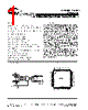
️· Product: The CY2DP3120 is a high-speed differential clock/data fanout buffer. It takes a single differential clock or data signal and distributes it to multiple differential outputs.
️· Application: Primarily used in systems requiring the distribution of clock or data signals in high-speed digital designs, often found in communication systems, networking equipment, and other high-performance applications.
️· Key Features:
- 1:20 Fanout (one input to twenty outputs).
- Supports PECL (Positive Emitter-Coupled Logic) and LVPECL (Low-Voltage PECL) signaling.
- Multiple output termination options for various interfaces.
- Low skew and jitter.
- Various package options (TQFP).
2. Electrical Characteristics:
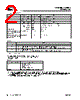
️· Supply Voltages: Supports various supply voltages, optimized for PECL and LVPECL operation.
️· Input Levels: Defined input voltage thresholds for PECL and LVPECL.
️· Output Levels: Specifies the output voltage levels for PECL and LVPECL.
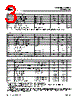
️· Timing Characteristics: Includes:
- Propagation Delay (TPLH, TPHL): Critical for high-speed operation; specifies the delay between input and output transitions.
- Output Skew: Measures the difference in propagation delay between multiple outputs, important for maintaining data integrity.
- Jitter: The variation in the timing of the signal.
️· Termination: Document provides diagrams and notes on termination techniques for PECL/ECL to LVDS interfaces.
3. Functionality & Modes of Operation:
️· Differential Signaling: The CY2DP3120 works with differential signals, which are more robust to noise than single-ended signals.
️· Termination: Proper termination of the outputs is crucial for signal integrity and to prevent reflections. The datasheet details various termination schemes.
4. Pinout and Package Information:
️· The device comes in a 52-pin TQFP package.
️· The pin configuration is clearly defined, indicating power supplies (VCC, VCCO), input pins, output pins, and control pins.
5. Ordering Information:
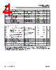
️· Several ordering options are provided, including different package types and temperature ranges (Industrial: -40°C to 85°C). Lead-free options are also available.
6. Diagrams & Figures:
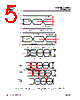
️· Input/Output Waveform Definitions: Illustrates the voltage levels and timing relationships for PECL and LVPECL signals.
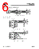
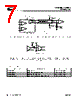
️· Termination Diagrams: Provides guidance on how to terminate PECL/ECL signals for various interfaces.
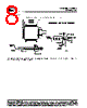
️· Package Diagram: Shows the physical dimensions and pin assignments of the TQFP package.
7. Revision History:
️· The document has gone through several revisions to correct errors, add information, and update specifications. The most recent revision is Rev. C.
In simpler terms:
Imagine you have a single heartbeat (clock signal) that needs to be felt in 20 different locations. This chip acts like a signal distributor, accurately replicating and sending that heartbeat to all 20 points, making sure they all feel it at the same time (low skew) and with minimal distortion (low jitter). It's designed for fast and reliable data transmission in electronics.
1. Overview & Purpose:
️· Product: The CY2DP3120 is a high-speed differential clock/data fanout buffer. It takes a single differential clock or data signal and distributes it to multiple differential outputs.
️· Application: Primarily used in systems requiring the distribution of clock or data signals in high-speed digital designs, often found in communication systems, networking equipment, and other high-performance applications.
️· Key Features:
- 1:20 Fanout (one input to twenty outputs).
- Supports PECL (Positive Emitter-Coupled Logic) and LVPECL (Low-Voltage PECL) signaling.
- Multiple output termination options for various interfaces.
- Low skew and jitter.
- Various package options (TQFP).
2. Electrical Characteristics:
️· Supply Voltages: Supports various supply voltages, optimized for PECL and LVPECL operation.
️· Input Levels: Defined input voltage thresholds for PECL and LVPECL.
️· Output Levels: Specifies the output voltage levels for PECL and LVPECL.
️· Timing Characteristics: Includes:
- Propagation Delay (TPLH, TPHL): Critical for high-speed operation; specifies the delay between input and output transitions.
- Output Skew: Measures the difference in propagation delay between multiple outputs, important for maintaining data integrity.
- Jitter: The variation in the timing of the signal.
️· Termination: Document provides diagrams and notes on termination techniques for PECL/ECL to LVDS interfaces.
3. Functionality & Modes of Operation:
️· Differential Signaling: The CY2DP3120 works with differential signals, which are more robust to noise than single-ended signals.
️· Termination: Proper termination of the outputs is crucial for signal integrity and to prevent reflections. The datasheet details various termination schemes.
4. Pinout and Package Information:
️· The device comes in a 52-pin TQFP package.
️· The pin configuration is clearly defined, indicating power supplies (VCC, VCCO), input pins, output pins, and control pins.
5. Ordering Information:
️· Several ordering options are provided, including different package types and temperature ranges (Industrial: -40°C to 85°C). Lead-free options are also available.
6. Diagrams & Figures:
️· Input/Output Waveform Definitions: Illustrates the voltage levels and timing relationships for PECL and LVPECL signals.
️· Termination Diagrams: Provides guidance on how to terminate PECL/ECL signals for various interfaces.
️· Package Diagram: Shows the physical dimensions and pin assignments of the TQFP package.
7. Revision History:
️· The document has gone through several revisions to correct errors, add information, and update specifications. The most recent revision is Rev. C.
In simpler terms:
Imagine you have a single heartbeat (clock signal) that needs to be felt in 20 different locations. This chip acts like a signal distributor, accurately replicating and sending that heartbeat to all 20 points, making sure they all feel it at the same time (low skew) and with minimal distortion (low jitter). It's designed for fast and reliable data transmission in electronics.
| Part No. | CY2DP3120AXIT |
| Manufacturer | CYPRESS |
| Size | 193 Kbytes |
| Pages | 9 pages |
| Description | 1:20 Differential Clock/Data Fanout Buffer |
| ALLDATASHEET é útil para você? [ DONATE ] |
Sobre Alldatasheet | Publicidade | Contato conosco | Privacy Policy | Link para a ficha técnica | roca de Link | Lista de Fabricantes All Rights Reserved©Alldatasheet.com |
| Russian : Alldatasheetru.com | Korean : Alldatasheet.co.kr | Spanish : Alldatasheet.es | French : Alldatasheet.fr | Italian : Alldatasheetit.com Portuguese : Alldatasheetpt.com | Polish : Alldatasheet.pl | Vietnamese : Alldatasheet.vn Indian : Alldatasheet.in | Mexican : Alldatasheet.com.mx | British : Alldatasheet.co.uk | New Zealand : Alldatasheet.co.nz |
|
Family Site : ic2ic.com |
icmetro.com |
 Portuguese ▼
  English
 Chinese
 German
 Japanese
 Russian
 Korean
 Spanish
 French
 Italian
 Polish
 Vietnamese
 Indian
 Mexican
 British
 New Zealand